DAC39J84IAAV OverviewThere is a 144-FBGA, FCBGA package that includes this component. It is powered from a supply voltage of 3.3V. The Surface Mount-slot on the development board allows you to attach the FPGA module. While operating, the operating temperature should be kept within a range of -40°C~85°C. As a space-saving measure, this FPGA model is contained within Tray. Total terminations are 144. In order to find related parts, you can use its base part number DAC39J84. It has a total of 144 pins that are designed for it. Providing that this FPGA is mounted in Surface Mount, it will be able to perform according to its specifications in a flawless manner. Designers can fully utili3.3Ve its flexibility with 3.3V supply voltage. As far as the pin count is concerned, it has 144 pins. The maximum supply voltage it supports is 3.45V. With a minimum supply voltage of 3.15V, it is able to function.
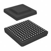
DAC39J84IAAV Features144-FBGA, FCBGA package
144 pin count
144 pins
DAC39J84IAAV ApplicationsThere are a lot of Texas Instruments
DAC39J84IAAV Digital to Analog Converters (DAC) applications.
Display Electronics
Data Acquisition Systems
Calibration
Motor Control
Data Distribution System
Digital Potentiometer
Software Radio
Wireless infrastructure:
WCDMA, CDMA2000, TD-SCDMA, WiMAX
Wideband communications:
| Lifecycle Status | ACTIVE (Last Updated: 2 days ago) |
| Factory Lead Time | 6 Weeks |
| Contact Plating | Copper, Silver, Tin |
| Mount | Surface Mount |
| Mounting Type | Surface Mount |
| Package / Case | 144-FBGA, FCBGA |
| Number of Pins | 144 |
| Operating Temperature | -40°C~85°C |
| Packaging | Tray |
| JESD-609 Code | e1 |
| Pbfree Code | yes |
| Part Status | Active |
| Moisture Sensitivity Level (MSL) | 3 (168 Hours) |
| Number of Terminations | 144 |
| ECCN Code | EAR99 |
| Terminal Finish | Tin/Silver/Copper (Sn/Ag/Cu) |
| Terminal Position | BOTTOM |
| Terminal Form | BALL |
| Number of Functions | 1 |
| Supply Voltage | 3.3V |
| Terminal Pitch | 0.8mm |
| Base Part Number | DAC39J84 |
| Pin Count | 144 |
| Output Type | Current - Unbuffered |
| Operating Supply Voltage | 3.3V |
| Max Supply Voltage | 3.45V |
| Min Supply Voltage | 3.15V |
| Number of Bits | 16 |
| Architecture | Current Source |
| Converter Type | D/A CONVERTER |
| Reference Type | External, Internal |
| Data Interface | JESD204B |
| Differential Output | Yes |
| Resolution | 2 B |
| Sampling Rate | 2800 MHz |
| Voltage - Supply, Analog | 3.15V~3.45V |
| Voltage - Supply, Digital | 0.85V~1.05V |
| Settling Time | 10ns (Typ) |
| Power Consumption | 1.62W |
| Integral Nonlinearity (INL) | 6 LSB |
| Input Bit Code | OFFSET BINARY, 2'S COMPLEMENT BINARY |
| Conversion Rate | 2.8 Gsps |
| INL/DNL (LSB) | ±6, ±4 |
| Input Format | PARALLEL, WORD |
| Number of D/A Converters | 4 |
| Analog Output Voltage-Max | 0.6V |
| Analog Output Voltage-Min | -0.5V |
| Height | 1.94mm |
| Length | 10mm |
| Width | 10mm |
| Thickness | 1.45mm |
| RoHS Status | ROHS3 Compliant |
| Lead Free | Lead Free |


 +8613715157867