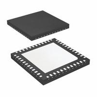
9DBU0841AKILF OverviewLocated in the Tray package, it can be accessed. 48-VFQFN Exposed Pad comes with the case. The mounting type to use is Surface Mount. As of right 1w, the device has 1. There is a maximum frequency for normaloperation of 167MHz. Clock program is possible to adjust the operating temperature range of -40°C~85°C. There is a possibility of the component supplying a voltage of 1.425V~1.575V. Component PCI Express (PCIe) serves the main purpose. In this case, LP-HCSL is meant to be the output.
9DBU0841AKILF FeaturesMounting Type: Surface Mount
Include 1 Circuits
run the output at th range of LP-HCSL
9DBU0841AKILF ApplicationsThere are a lot of Renesas Electronics America Inc.
9DBU0841AKILF application specific timer applications.
PCI Express 2.0/3.0
Broadcast video/audio timing
Processor and FPGA clocking
Any-frequency clock conversion
MSAN/DSLAM/PON
Fibre Channel, SAN
Telecom line cards
1 GbE and 10 GbE
Servers, Storage, Search Acceleration
Ethernet Switches, Routers
| Factory Lead Time | 12 Weeks |
| Mounting Type | Surface Mount |
| Package / Case | 48-VFQFN Exposed Pad |
| Operating Temperature | -40°C~85°C |
| Packaging | Tray |
| Part Status | Active |
| Moisture Sensitivity Level (MSL) | 3 (168 Hours) |
| Voltage - Supply | 1.425V~1.575V |
| Output | LP-HCSL |
| Number of Circuits | 1 |
| Frequency (Max) | 167MHz |
| Input | HCSL |
| Ratio - Input:Output | 1:8 |
| PLL | Yes |
| Differential - Input:Output | Yes/Yes |
| Main Purpose | PCI Express (PCIe) |
| RoHS Status | ROHS3 Compliant |
| Factory Lead Time | 7 Weeks |
| Contact Plating | Tin |
| Mount | Surface Mount |
| Number of Pins | 48 |
| Supplier Device Package | 48-VFQFPN (6x6) |
| Other Names | 800-2807 |
| Frequency - Max | 167MHz |
| Published | 2006 |
| Operating Temperature | -40°C ~ 85°C |
| Series | - |
| JESD-609 Code | e3 |
| Pbfree Code | yes |
| Number of Terminations | 48 |
| ECCN Code | EAR99 |
| Max Operating Temperature | 85°C |
| Min Operating Temperature | -40°C |
| Voltage - Supply | 1.425 V ~ 1.575 V |
| Terminal Position | QUAD |
| Terminal Form | NO LEAD |
| Peak Reflow Temperature (Cel) | 260 |
| Number of Functions | 1 |
| Supply Voltage | 1.5V |
| Terminal Pitch | 0.4mm |
| Time@Peak Reflow Temperature-Max (s) | NOT SPECIFIED |
| Pin Count | 48 |
| Number of Outputs | 2 |
| Operating Supply Voltage | 1.5V |
| Temperature Grade | INDUSTRIAL |
| Max Supply Voltage | 1.575V |
| Min Supply Voltage | 1.425V |
| Power Dissipation-Max | 53mW |
| Operating Supply Current | 9mA |
| Family | 9DBU |
| Logic IC Type | PLL BASED CLOCK DRIVER |
| Max Duty Cycle | 55 % |
| Same Edge Skew-Max (tskwd) | 0.075 ns |
| Height | 900μm |
| Length | 6mm |
| Width | 6mm |
| Thickness | 900μm |
| RoHS Status | RoHS Compliant |
| Lead Free | Lead Free |

 9DBU0841AKILF Datasheet
 +8613715157867