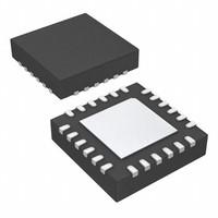
9DBV0231AKLF OverviewIn order to ensure the safety and security of the product, it is packaged in a case with a QFN-serial number. This termination has 24 terminations. 1.8V is the voltage provided by this part. 260 runs using this part's peak reflow temperature. In the device, there are 1. Clock program is normalfor the operation frequency to be 137.5MHz. A total of 2006 publications have been made of the part. With Surface Mount, it is recommended that it be mounted. A device with 24 pins is designed. The board contains 24 pins. Minimum working temperature must not be below 0°C. Temperatures below 70°C should be used. In this device, 2 outputs can be maintained. The part is operated under 1.9V in terms of voltage supply. Circuits application is imperative that the device is always supplied wCircuits applicationh voltage greater than 1.7V. If you choose a part from the 9DBV family, you can find parts that are related to that part. There are PLL BASED CLOCK DRIVER logic IC types used in it.
9DBV0231AKLF FeaturesPeak Reflow Temperature (Cel): 260
Include 1 Circuits
with 24 Pins
Logic IC Type: PLL BASED CLOCK DRIVER
9DBV0231AKLF ApplicationsThere are a lot of Integrated Device Technology (IDT)
9DBV0231AKLF application specific timer applications.
Processor and FPGA clocking
Any-frequency clock conversion
MSAN/DSLAM/PON
Fibre Channel, SAN
Telecom line cards
1 GbE and 10 GbE
Servers, Storage, Search Acceleration
Ethernet Switches, Routers
Small Cells, Mobile Backhaul/Fronthaul
Print Imaging
| Factory Lead Time | 7 Weeks |
| Contact Plating | Tin |
| Mount | Surface Mount |
| Package / Case | QFN |
| Number of Pins | 24 |
| Published | 2006 |
| JESD-609 Code | e3 |
| Pbfree Code | yes |
| Part Status | Active |
| Moisture Sensitivity Level (MSL) | 1 (Unlimited) |
| Number of Terminations | 24 |
| ECCN Code | EAR99 |
| Max Operating Temperature | 70°C |
| Min Operating Temperature | 0°C |
| Terminal Position | QUAD |
| Terminal Form | NO LEAD |
| Peak Reflow Temperature (Cel) | 260 |
| Number of Functions | 1 |
| Supply Voltage | 1.8V |
| Terminal Pitch | 0.5mm |
| Time@Peak Reflow Temperature-Max (s) | NOT SPECIFIED |
| Pin Count | 24 |
| Number of Outputs | 2 |
| Qualification Status | Not Qualified |
| Temperature Grade | COMMERCIAL |
| Number of Circuits | 1 |
| Max Supply Voltage | 1.9V |
| Min Supply Voltage | 1.7V |
| Nominal Supply Current | 25mA |
| Frequency (Max) | 137.5MHz |
| Family | 9DBV |
| Input | HCSL |
| Logic IC Type | PLL BASED CLOCK DRIVER |
| PLL | Yes |
| Prop. Delay@Nom-Sup | 5 ns |
| Same Edge Skew-Max (tskwd) | 0.05 ns |
| Length | 4mm |
| Width | 4mm |
| Thickness | 900μm |
| RoHS Status | RoHS Compliant |
| Lead Free | Lead Free |
| Factory Lead Time | 12 Weeks |
| Mounting Type | Surface Mount |
| Package / Case | 24-VFQFN Exposed Pad |
| Operating Temperature | 0°C~70°C |
| Packaging | Tube |
| Voltage - Supply | 1.7V~1.9V |
| Base Part Number | ICS9DBV0231 |
| Ratio - Input:Output | 1:2 |
| Differential - Input:Output | Yes/Yes |
| Main Purpose | Ethernet, PCI Express (PCIe) |
| RoHS Status | ROHS3 Compliant |

 9DBV0231AKLF Datasheet
 +8613715157867