ADCLK854BCPZ-REEL7 OverviewThere is a case option of 48-VFQFN Exposed Pad, CSP available for this clock divider. There is a Tape & Reel (TR) packaged with it. Normal operation is limited to 1.2GHz. 48 terminations have been recorded. With a supply voltage of 1.8V, high efficiency is possible. As far as I can tell, it is mounted by Surface Mount. Electronic parts classified as Fanout Buffer (Distribution), Multiplexer are considered to be safety components. It is recommended to set the temperature to -40°C~85°C so the system can perform reliably. In order for it to function, a power source of 1.71V~1.89V V must be available. A pin count of 48 can be found on it. As a result, the output is CMOS, LVDS. It is operated using the 48 pins. This is a member of the family of ADCLK854. There is a default setting of output 12. In order to achieve maximum efficiency, the supply voltage should be kept at 1.8V. The configuration is complete when 2 is input.
ADCLK854BCPZ-REEL7 Features48 terminations
The operating temperature of -40°C~85°C degrees
ADCLK854BCPZ-REEL7 ApplicationsThere are a lot of Analog Devices Inc.
ADCLK854BCPZ-REEL7 Clock Buffers & Drivers applications.
Clock signal duplication
Clock signal format conversion
Clock signal level shifting
High performance communication system
Data center
Cloud computing
Network
High speed industry
High-end consumer electronics
Data communication
| Lifecycle Status | PRODUCTION (Last Updated: 2 weeks ago) |
| Factory Lead Time | 8 Weeks |
| Contact Plating | Tin |
| Mounting Type | Surface Mount |
| Package / Case | 48-VFQFN Exposed Pad, CSP |
| Surface Mount | YES |
| Number of Pins | 48 |
| Operating Temperature | -40°C~85°C |
| Packaging | Tape & Reel (TR) |
| JESD-609 Code | e3 |
| Pbfree Code | no |
| Part Status | Active |
| Moisture Sensitivity Level (MSL) | 3 (168 Hours) |
| Number of Terminations | 48 |
| ECCN Code | EAR99 |
| Type | Fanout Buffer (Distribution), Multiplexer |
| Voltage - Supply | 1.71V~1.89V |
| Terminal Position | QUAD |
| Peak Reflow Temperature (Cel) | 260 |
| Number of Functions | 1 |
| Supply Voltage | 1.8V |
| Terminal Pitch | 0.5mm |
| Time@Peak Reflow Temperature-Max (s) | 40 |
| Base Part Number | ADCLK854 |
| Output | CMOS, LVDS |
| Pin Count | 48 |
| Number of Outputs | 12 |
| Operating Supply Voltage | 1.8V |
| Number of Circuits | 1 |
| Propagation Delay | 4.2 ns |
| Frequency (Max) | 1.2GHz |
| Number of Inputs | 2 |
| Input | CML, CMOS, HSTL, LVDS, LVPECL |
| Average Bias Current-Max (IIB) | 350μA |
| Ratio - Input:Output | 2:12 |
| Supply Voltage Limit-Max | 2V |
| Differential - Input:Output | Yes/Yes |
| Length | 7mm |
| Width | 7mm |
| Radiation Hardening | No |
| RoHS Status | ROHS3 Compliant |
| Lead Free | Contains Lead |
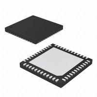

 ADCLK854BCPZ-REEL7 Datasheet
 +8613715157867