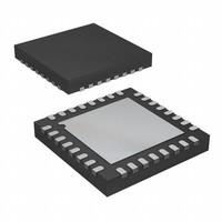
ADF4350BCPZ-RL OverviewAs a clock IC, PLLs is packaged using the Tape & Reel (TR) method. This clock generator is embedded in the 32-WFQFN Exposed Pad, CSP package. Under reflowing process, this clock generator ic is able to sustain a maximum temperature of 260. 32 terminations can be found in frequency synthesizer. Basically, a voltage of 3.3V should be applied to this electronic frequency generator. CMOS, TTL is designed as this clock generator's input. 1 circuits are implemented to access the electronic component's full performance. This clock-based frequency generator provides a frequency up to 4.4GHz Max. This component can be conveniently installed on the panel thanks to the Surface Mount. The maximal supply voltage this clock generator would take is 3.6V. The supply voltage for this frequency synthesizer should be kept above 3V for safety considerations. Clock PLL works with 3V~3.6V supply voltage provided. The ambient temperature should be set at -40°C~85°C, which is estimated by the test statistics. This is a clock generator compatible with Clock logic levels. This electronic component can be classified as a Fanout Distribution, Fractional N, Integer N, Clock/Frequency Synthesizer (RF). This clock-generating IC is a 32-bit device designed explicitly for microprocessors. According to the base part number ADF4350, its related parts can be found. There is an available 32 pin on the clock generators. RF synthesizers can handle voltages up to 3.3V. Clock PLL is facilitated with 4 signal outputs to magnify output frequency as high as possible. A supply current of 110mA needs to be provided to fully play RF synthesizer's function. The maximum supply current for this electronic frequency generator should not be in excess of 27mA.
ADF4350BCPZ-RL FeaturesAvailable in the 32-WFQFN Exposed Pad, CSP
Supply voltage of 3.3V
Operating supply voltage of 3.3V
ADF4350BCPZ-RL ApplicationsThere are a lot of Analog Devices Inc.
ADF4350BCPZ-RL Clock Generators applications.
Instrument
Automatic test equipment
Wide area power system
Digital circuits
Wireless base station for LTE, LTE-advanced
Picocells, femtocells and small cells
Sampling clocks for ADC and DAC
1 Gigabit Ethernet
10 Gigabit Ethernet
FPGA and processor clocks
| Lifecycle Status | PRODUCTION (Last Updated: 1 week ago) |
| Factory Lead Time | 14 Weeks |
| Contact Plating | Tin |
| Mount | Surface Mount |
| Mounting Type | Surface Mount |
| Package / Case | 32-WFQFN Exposed Pad, CSP |
| Number of Pins | 32 |
| Operating Temperature | -40°C~85°C |
| Packaging | Tape & Reel (TR) |
| JESD-609 Code | e3 |
| Pbfree Code | no |
| Part Status | Active |
| Moisture Sensitivity Level (MSL) | 3 (168 Hours) |
| Number of Terminations | 32 |
| ECCN Code | EAR99 |
| Type | Fanout Distribution, Fractional N, Integer N, Clock/Frequency Synthesizer (RF) |
| Voltage - Supply | 3V~3.6V |
| Terminal Position | QUAD |
| Terminal Form | NO LEAD |
| Peak Reflow Temperature (Cel) | 260 |
| Number of Functions | 1 |
| Supply Voltage | 3.3V |
| Terminal Pitch | 0.5mm |
| Time@Peak Reflow Temperature-Max (s) | 40 |
| Base Part Number | ADF4350 |
| Output | Clock |
| Pin Count | 32 |
| Number of Outputs | 4 |
| Qualification Status | Not Qualified |
| Operating Supply Voltage | 3.3V |
| Supply Voltage-Max (Vsup) | 3.6V |
| Supply Voltage-Min (Vsup) | 3V |
| Number of Circuits | 1 |
| Operating Supply Current | 110mA |
| Nominal Supply Current | 110mA |
| Frequency (Max) | 4.4GHz |
| Supply Current-Max (Isup) | 27mA |
| Input | CMOS, TTL |
| Ratio - Input:Output | 1:2 |
| PLL | Yes |
| Differential - Input:Output | No/No |
| Divider/Multiplier | Yes/Yes |
| Length | 5mm |
| Width | 5mm |
| RoHS Status | ROHS3 Compliant |
| Lead Free | Contains Lead |
