CDC516DGGR OverviewThis clock IC is packaged using the Tape & Reel (TR) method. The 48-TFSOP (0.240, 6.10mm Width) package includes this clock generator. In the reflowing process, this clock generator ic is able to maintain a maximum temperature of 260. In it, there are 48 terminations to be found. This time clock generator should be voltaged at 3.3V. A clock generator's input is called LVTTL and it is designed as the input for this clock generator. For full access to the electronic component's capabilities, 1 circuits are implemented. With the Surface Mount, it is easy to install this electric component on the panel. Clock generators can take up to 3.6V of power as a maximum supply voltageThis frequency synthesizer requires a supply voltage above 3V to be safe. This clock PLL works with a supply voltage of 3V~3.6V. Using the test statistics, it is estimated that the ambient temperature should be set to 0°C~70°C. A PLL Clock Driver is a classification for the electronic part in question. Microprocessors are specifically designed to use this clock-generating IC, which has a 48-bit output. This part number CDC516 is related to the following electrical components. PF synthesizers is equipped with 48 pins. PLL clock can handle a voltage of 3.3V as its supply voltage. Clock PLL has 16 signal outputs to maximi16e output frequency. There is a low timing skew at 0.2 nsmax with this RF synthesizer. A search for the 516 family will yield similar electronic components. When operated at 125MHz, frequency synthesizer achieves high efficiency. As a result, the load capacitance of this PLL is 30pF. A clock generator ic such as this would be well suited to the TR package.
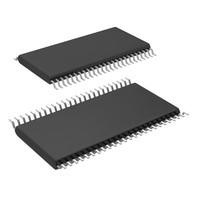
CDC516DGGR FeaturesAvailable in the 48-TFSOP (0.240, 6.10mm Width)
Supply voltage of 3.3V
Operating supply voltage of 3.3V
Load capacitance of 30pF
CDC516DGGR ApplicationsThere are a lot of Texas Instruments
CDC516DGGR Clock Generators applications.
Digital circuits
Wireless base station for LTE, LTE-advanced
Picocells, femtocells and small cells
Sampling clocks for ADC and DAC
1 Gigabit Ethernet
10 Gigabit Ethernet
FPGA and processor clocks
Line cards used in telephone exchange
Fiber Channel
PCI express cards
| Lifecycle Status | ACTIVE (Last Updated: 5 days ago) |
| Factory Lead Time | 6 Weeks |
| Contact Plating | Gold |
| Mount | Surface Mount |
| Mounting Type | Surface Mount |
| Package / Case | 48-TFSOP (0.240, 6.10mm Width) |
| Number of Pins | 48 |
| Weight | 223.195796mg |
| Operating Temperature | 0°C~70°C |
| Packaging | Tape & Reel (TR) |
| JESD-609 Code | e4 |
| Pbfree Code | yes |
| Part Status | Active |
| Moisture Sensitivity Level (MSL) | 2 (1 Year) |
| Number of Terminations | 48 |
| ECCN Code | EAR99 |
| Type | PLL Clock Driver |
| Packing Method | TR |
| Voltage - Supply | 3V~3.6V |
| Terminal Position | DUAL |
| Terminal Form | GULL WING |
| Peak Reflow Temperature (Cel) | 260 |
| Number of Functions | 1 |
| Supply Voltage | 3.3V |
| Terminal Pitch | 0.5mm |
| Frequency | 125MHz |
| Base Part Number | CDC516 |
| Pin Count | 48 |
| Number of Outputs | 16 |
| Operating Supply Voltage | 3.3V |
| Supply Voltage-Max (Vsup) | 3.6V |
| Supply Voltage-Min (Vsup) | 3V |
| Number of Circuits | 1 |
| Load Capacitance | 30pF |
| Nominal Supply Current | 20μA |
| Family | 516 |
| Input | LVTTL |
| Ratio - Input:Output | 1:16 |
| Max I(ol) | 0.02 A |
| PLL | Yes with Bypass |
| Differential - Input:Output | No/No |
| Power Supply Current-Max (ICC) | 0.02mA |
| Same Edge Skew-Max (tskwd) | 0.2 ns |
| Height | 1.2mm |
| Length | 12.5mm |
| Width | 6.1mm |
| Thickness | 1.15mm |
| Radiation Hardening | No |
| RoHS Status | ROHS3 Compliant |
| Lead Free | Lead Free |


 +8613715157867