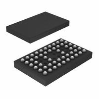
CDCU877ZQLT OverviewLocated in the Tape & Reel (TR) package, it can be accessed. 52-VFBGA comes with the case. The mounting type to use is Surface Mount. 52 terminations are found in it. Voltage 1.8V is provided by the part. To run 260, we utilize this part's peak reflow temperature. As of right 1w, the device has 1. Clock program is possible to adjust the operating temperature range of -40°C~85°C. There is a possibility of the component supplying a voltage of 1.7V~1.9V. Component Memory, DDR2 serves the main purpose. You will be able to search for information based on CDCU877. Circuits application is recommended to mount Circuits application wCircuits applicationh Surface Mount. 52 pins are provided on the device. The board includes 52 pins. 1.8V is the recommended supply voltage. 10 outputs are possible on the device. Circuits application is possible to search for related parts based on the 877 family of parts. PLL BASED CLOCK DRIVER logic ICs are used. Circuits application is incredibly efficient when operating at 400MHz.
CDCU877ZQLT FeaturesMounting Type: Surface Mount
Peak Reflow Temperature (Cel): 260
Include 1 Circuits
with 52 Pins
operate supply voltage at the range of 1.8V
Logic IC Type: PLL BASED CLOCK DRIVER
CDCU877ZQLT ApplicationsThere are a lot of Texas Instruments
CDCU877ZQLT application specific timer applications.
PCI Express 2.0/3.0
Broadcast video/audio timing
Processor and FPGA clocking
Any-frequency clock conversion
MSAN/DSLAM/PON
Fibre Channel, SAN
Telecom line cards
1 GbE and 10 GbE
Servers, Storage, Search Acceleration
Ethernet Switches, Routers
| Contact Plating | Copper, Silver, Tin |
| Mount | Surface Mount |
| Mounting Type | Surface Mount |
| Package / Case | 52-VFBGA |
| Number of Pins | 52 |
| Weight | 57.804678mg |
| Operating Temperature | -40°C~85°C |
| Packaging | Tape & Reel (TR) |
| JESD-609 Code | e1 |
| Pbfree Code | yes |
| Part Status | Obsolete |
| Moisture Sensitivity Level (MSL) | 2 (1 Year) |
| Number of Terminations | 52 |
| Termination | SMD/SMT |
| ECCN Code | EAR99 |
| Terminal Finish | Tin/Silver/Copper (Sn/Ag/Cu) |
| Packing Method | TR |
| Voltage - Supply | 1.7V~1.9V |
| Terminal Position | BOTTOM |
| Terminal Form | BALL |
| Peak Reflow Temperature (Cel) | 260 |
| Number of Functions | 1 |
| Supply Voltage | 1.8V |
| Terminal Pitch | 0.65mm |
| Frequency | 400MHz |
| Base Part Number | CDCU877 |
| Pin Count | 52 |
| Number of Outputs | 10 |
| Operating Supply Voltage | 1.8V |
| Number of Circuits | 1 |
| Nominal Supply Current | 500μA |
| Family | 877 |
| Output Characteristics | 3-STATE |
| Input | SSTL-18 |
| Ratio - Input:Output | 1:10 |
| Logic IC Type | PLL BASED CLOCK DRIVER |
| Max I(ol) | 0.009 A |
| PLL | Yes |
| Differential - Input:Output | Yes/Yes |
| Main Purpose | Memory, DDR2 |
| Input Current | 250μA |
| fmax-Min | 340 MHz |
| Same Edge Skew-Max (tskwd) | 0.035 ns |
| Height | 1mm |
| Length | 7mm |
| Width | 4.5mm |
| Thickness | 750μm |
| REACH SVHC | No SVHC |
| Radiation Hardening | No |
| RoHS Status | ROHS3 Compliant |
| Lead Free | Lead Free |

 CDCU877ZQLT Datasheet
 +8613715157867