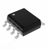
CY2DP1502SXIT OverviewThere is a case available for the cut smart buffer in 8-SOIC (0.154, 3.90mm Width). This package is packaged in the form of a Tape & Reel (TR). For normal operation, 1.5GHz is the maximum value. It has 8 terminations in it, which means that it is terminated. Supply voltages of 2.5V are capable of achieving high efficiency. In this case, it will be mounted by Surface Mount. A classification of Fanout Buffer (Distribution) is assigned to this electronic part. Setting the temperature to -40°C~85°C will ensure reliable performance. Ideally, it should be able to operate from 2.375V~3.465V volts. There are 8 pins on the clock buffer. There is a value of LVPECL as the output. During operation, 8 pins are used. A member of the S family, this clock buffer is a digital camera. As a default, it is set to output 2.
CY2DP1502SXIT Features8 terminations
The operating temperature of -40°C~85°C degrees
CY2DP1502SXIT ApplicationsThere are a lot of Cypress Semiconductor Corp
CY2DP1502SXIT Clock Buffers & Drivers applications.
Clock signal format conversion
Clock signal level shifting
High performance communication system
Data center
Cloud computing
Network
High speed industry
High-end consumer electronics
Data communication
Telecommunications
| Factory Lead Time | 15 Weeks |
| Mounting Type | Surface Mount |
| Package / Case | 8-SOIC (0.154, 3.90mm Width) |
| Surface Mount | YES |
| Number of Pins | 8 |
| Operating Temperature | -40°C~85°C |
| Packaging | Tape & Reel (TR) |
| Published | 2002 |
| JESD-609 Code | e4 |
| Pbfree Code | yes |
| Part Status | Obsolete |
| Moisture Sensitivity Level (MSL) | 3 (168 Hours) |
| Number of Terminations | 8 |
| ECCN Code | EAR99 |
| Type | Fanout Buffer (Distribution) |
| Terminal Finish | Nickel/Palladium/Gold (Ni/Pd/Au) |
| Voltage - Supply | 2.375V~3.465V |
| Terminal Position | DUAL |
| Terminal Form | GULL WING |
| Peak Reflow Temperature (Cel) | 260 |
| Number of Functions | 1 |
| Supply Voltage | 2.5V |
| Time@Peak Reflow Temperature-Max (s) | 20 |
| Output | LVPECL |
| Pin Count | 8 |
| Number of Outputs | 2 |
| Qualification Status | Not Qualified |
| Number of Circuits | 1 |
| Propagation Delay | 480 ps |
| Frequency (Max) | 1.5GHz |
| Family | S |
| Input | CML, HCSL, LVDS, LVPECL |
| Ratio - Input:Output | 1:2 |
| Differential - Input:Output | Yes/Yes |
| Max Duty Cycle | 52 % |
| Duty Cycle | 52 % |
| RoHS Status | ROHS3 Compliant |
| Lead Free | Lead Free |


 +8613715157867