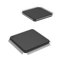
LCMXO1200C-4TN100I OverviewIn the package 100-LQFP, this product is provided. Fpga chips consists of FLASH PLD elements. A total of 73 I/Os are programmed to ensure a more coherent data transfer. The basic building blocks of logic contain 1200 logic elements/cells. Supply voltage is 1.8V volts. By attaching the Surface Mount connector, you can use this FPGA module with your development board. With a supply voltage of 1.71V~3.465V, this device operates with ease. This is a type of FPGA that is part of the MachXO series of FPGAs. Fpga chips is necessary to keep the operating temperature wFpga chipshin -40°C~100°C TJ when the device is operating. In this device, 73 outputs are incorporated in order to provide you with maximum flexibility. As a result of space limitations, this FPGA model has been included in Tray. In total, the terminations of this piece are 100. Fpga electronics is worth mentioning that this device provides 9421 bfpga electronics s of RAM. LCMXO1200 is the base part number that can be used to identify related parts. The device has 100 pins which are included in the design. The FPGA is built as an array of 150 latches or CLBs. I think, as long as this FPGA is mounted in Surface Mount, it could perform excellently according to its specifications as long as you mount it in Surface Mount. In operation with 3.3V, designers can take advantage of its flexibility to the fullest extent. I am going to present you with a device that is equipped with 100 pins. In fact, this FPGA is capable of reaching a speed of 550MHz. There is a 21mA supply current used in its operation. In addition, it has a feature called IT CAN ALSO OPERATE AT 2.5V AND 3.3V. There are a total of 7 dedicated inputs that allow input signals to be detected the status of each input. In this device, the main building blocks of a CPLD are 600 macro cells, which serve as the main components of the device. In the SRAM memory, data is stored safely and resource conflicts are avoided.
LCMXO1200C-4TN100I Features73 I/Os
Up to 9421 RAM bits
100 LABs/CLBs
LCMXO1200C-4TN100I ApplicationsThere are a lot of Lattice Semiconductor Corporation
LCMXO1200C-4TN100I FPGAs applications.
Voice recognition
Cryptography
Filtering and communication encoding
Aerospace and Defense
Medical Electronics
Audio
Automotive
Consumer Electronics
Distributed Monetary Systems
Data Center
| Factory Lead Time | 8 Weeks |
| Mount | Surface Mount |
| Mounting Type | Surface Mount |
| Package / Case | 100-LQFP |
| Number of Pins | 100 |
| Operating Temperature | -40°C~100°C TJ |
| Packaging | Tray |
| Series | MachXO |
| Published | 2000 |
| JESD-609 Code | e3 |
| Pbfree Code | yes |
| Part Status | Active |
| Moisture Sensitivity Level (MSL) | 3 (168 Hours) |
| Number of Terminations | 100 |
| ECCN Code | EAR99 |
| Terminal Finish | Matte Tin (Sn) |
| Additional Feature | IT CAN ALSO OPERATE AT 2.5V AND 3.3V |
| HTS Code | 8542.39.00.01 |
| Voltage - Supply | 1.71V~3.465V |
| Terminal Position | QUAD |
| Terminal Form | GULL WING |
| Peak Reflow Temperature (Cel) | 260 |
| Supply Voltage | 1.8V |
| Terminal Pitch | 0.5mm |
| Time@Peak Reflow Temperature-Max (s) | 30 |
| Base Part Number | LCMXO1200 |
| Pin Count | 100 |
| Number of Outputs | 73 |
| Operating Supply Voltage | 3.3V |
| Operating Supply Current | 21mA |
| Number of I/O | 73 |
| Nominal Supply Current | 21mA |
| Memory Type | SRAM |
| Propagation Delay | 4.4 ns |
| Turn On Delay Time | 4.4 ns |
| Programmable Logic Type | FLASH PLD |
| Number of Logic Elements/Cells | 1200 |
| Total RAM Bits | 9421 |
| Max Frequency | 550MHz |
| Number of LABs/CLBs | 150 |
| Output Function | MACROCELL |
| Number of Macro Cells | 600 |
| Number of Dedicated Inputs | 7 |
| Length | 14mm |
| Height Seated (Max) | 1.6mm |
| Width | 14mm |
| Radiation Hardening | No |
| RoHS Status | ROHS3 Compliant |
| Lead Free | Lead Free |

 LCMXO1200C-4TN100I Datasheet
 +8613715157867