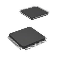
LCMXO1200C-5TN100C OverviewFpga chips is supplied in the 100-LQFP package. This kind of FPGA is composed of FLASH PLD. Fpga chips is programmed wFpga chipsh 73 I/Os for transferring data in a more coherent manner. There are 1200 logic elements/cells to form a fundamental building block. Fpga chips is powered from a supply voltage of 1.8V. This FPGA module can be attached to the development board with a Surface Mount. Fpga chips operates wFpga chipsh a supply voltage of 1.71V~3.465V. It is a type of FPGA belonging to the MachXO seies. The operating temperature should be kept at 0°C~85°C TJ when operating. There are 73 outputs incorporated in this device. This FPGA model is contained in Tray for space saving. Fpga chips is designed wFpga chipsh 100 terminations. The RAM bits that this device offer is 9421. Its base part number LCMXO1200 can be used to find related parts. Fpga electronics is designed wfpga electronics h 100 pins. This FPGA is built as an array of 150 LABs/CLBs. As long as this FPGA is mounted in Surface Mount, it could work fantastically according to its specifications. When operating with the supply voltage of 3.3V, designers can fully make use of its flexibility. Fpga semiconductor is equipped wfpga semiconductorh 100 pin count. Its basic building block is composed of 264 logic blocks (LABs). Typically, fpga semiconductor uses a crystal oscillating at 420MHz . The supply current used for its operation is 21mA. Fpga semiconductor is also characteriIT CAN ALSO OPERATE AT 2.5V AND 3.3Ved by a feature called IT CAN ALSO OPERATE AT 2.5V AND 3.3V. There are 7 dedicated inputs used to detect the status of input signals. In this device, 600 Macro cells are the main building blocks of a CPLD. The SRAM memory is adopted for storing data and avoiding resource conflicts.
LCMXO1200C-5TN100C Features73 I/Os
Up to 9421 RAM bits
100 LABs/CLBs
264 logic blocks (LABs)
LCMXO1200C-5TN100C ApplicationsThere are a lot of Lattice Semiconductor Corporation
LCMXO1200C-5TN100C FPGAs applications.
Digital signal processing
Bioinformatics
Device controllers
Software-defined radio
Random logic
ASIC prototyping
Medical imaging
Computer hardware emulation
Integrating multiple SPLDs
Voice recognition
| Factory Lead Time | 8 Weeks |
| Mount | Surface Mount |
| Mounting Type | Surface Mount |
| Package / Case | 100-LQFP |
| Number of Pins | 100 |
| Weight | 657.000198mg |
| Operating Temperature | 0°C~85°C TJ |
| Packaging | Tray |
| Series | MachXO |
| Published | 2000 |
| JESD-609 Code | e3 |
| Pbfree Code | yes |
| Part Status | Active |
| Moisture Sensitivity Level (MSL) | 3 (168 Hours) |
| Number of Terminations | 100 |
| ECCN Code | EAR99 |
| Terminal Finish | Matte Tin (Sn) |
| Additional Feature | IT CAN ALSO OPERATE AT 2.5V AND 3.3V |
| HTS Code | 8542.39.00.01 |
| Voltage - Supply | 1.71V~3.465V |
| Terminal Position | QUAD |
| Terminal Form | GULL WING |
| Peak Reflow Temperature (Cel) | 260 |
| Supply Voltage | 1.8V |
| Terminal Pitch | 0.5mm |
| Time@Peak Reflow Temperature-Max (s) | 30 |
| Base Part Number | LCMXO1200 |
| Pin Count | 100 |
| Number of Outputs | 73 |
| Operating Supply Voltage | 3.3V |
| Operating Supply Current | 21mA |
| Number of I/O | 73 |
| Memory Type | SRAM |
| Clock Frequency | 420MHz |
| Propagation Delay | 3.6 ns |
| Turn On Delay Time | 3.6 ns |
| Programmable Logic Type | FLASH PLD |
| Number of Logic Elements/Cells | 1200 |
| Total RAM Bits | 9421 |
| Number of LABs/CLBs | 150 |
| Number of Logic Blocks (LABs) | 264 |
| Output Function | MACROCELL |
| Number of Macro Cells | 600 |
| Number of Dedicated Inputs | 7 |
| Height | 1.4mm |
| Length | 14mm |
| Width | 14mm |
| Radiation Hardening | No |
| RoHS Status | ROHS3 Compliant |
| Lead Free | Lead Free |

 LCMXO1200C-5TN100C Datasheet
 +8613715157867