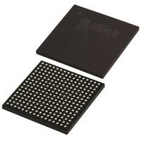
LCMXO2-1200UHC-4FTG256C OverviewIn the package 256-LBGA, this product is provided. Fpga chips consists of FIELD PROGRAMMABLE GATE ARRAY elements. A total of 206 I/Os are programmed to ensure a more coherent data transfer. The basic building blocks of logic contain 1280 logic elements/cells. Supply voltage is 2.5V volts. By attaching the Surface Mount connector, you can use this FPGA module with your development board. With a supply voltage of 2.375V~3.465V, this device operates with ease. This is a type of FPGA that is part of the MachXO2 series of FPGAs. Fpga chips is necessary to keep the operating temperature wFpga chipshin 0°C~85°C TJ when the device is operating. In this device, 207 outputs are incorporated in order to provide you with maximum flexibility. As a result of space limitations, this FPGA model has been included in Tray. In total, the terminations of this piece are 256. Fpga electronics is worth mentioning that this device provides 75776 bfpga electronics s of RAM. LCMXO2-1200 is the base part number that can be used to identify related parts. The RAM si9.3kBe of this FPGA module reaches 9.3kB so as to guarantee the normal operation of the program during operation. The device has 256 pins which are included in the design. The FPGA is built as an array of 160 latches or CLBs. I think, as long as this FPGA is mounted in Surface Mount, it could perform excellently according to its specifications as long as you mount it in Surface Mount. In operation with 2.5V, designers can take advantage of its flexibility to the fullest extent. This is a battery operated device that operates on 2.5/3.3V. I am going to present you with a device that is equipped with 256 pins. There is a memory of 20.5kB embedded inside this FPGA module that can be used to store programs and data. The system operates at a frequency of 269MHz in order to achieve maximum efficiency. There is a 56μA supply current used in its operation. In this device, the main building blocks of a CPLD are 640 macro cells, which serve as the main components of the device. In the FLASH memory, data is stored safely and resource conflicts are avoided.
LCMXO2-1200UHC-4FTG256C Features206 I/Os
Up to 75776 RAM bits
256 LABs/CLBs
Operating from a frequency of 269MHz
LCMXO2-1200UHC-4FTG256C ApplicationsThere are a lot of Lattice Semiconductor Corporation
LCMXO2-1200UHC-4FTG256C FPGAs applications.
Voice recognition
Cryptography
Filtering and communication encoding
Aerospace and Defense
Medical Electronics
Audio
Automotive
Consumer Electronics
Distributed Monetary Systems
Data Center
| Factory Lead Time | 8 Weeks |
| Mount | Surface Mount |
| Mounting Type | Surface Mount |
| Package / Case | 256-LBGA |
| Number of Pins | 256 |
| Operating Temperature | 0°C~85°C TJ |
| Packaging | Tray |
| Series | MachXO2 |
| Published | 2012 |
| JESD-609 Code | e1 |
| Pbfree Code | yes |
| Part Status | Active |
| Moisture Sensitivity Level (MSL) | 3 (168 Hours) |
| Number of Terminations | 256 |
| ECCN Code | EAR99 |
| Terminal Finish | Tin/Silver/Copper (Sn/Ag/Cu) |
| HTS Code | 8542.39.00.01 |
| Voltage - Supply | 2.375V~3.465V |
| Terminal Position | BOTTOM |
| Terminal Form | BALL |
| Peak Reflow Temperature (Cel) | 260 |
| Supply Voltage | 2.5V |
| Terminal Pitch | 1mm |
| Reach Compliance Code | not_compliant |
| Frequency | 269MHz |
| Time@Peak Reflow Temperature-Max (s) | 30 |
| Base Part Number | LCMXO2-1200 |
| Pin Count | 256 |
| Number of Outputs | 207 |
| Qualification Status | Not Qualified |
| Operating Supply Voltage | 2.5V |
| Power Supplies | 2.5/3.3V |
| Memory Size | 20.5kB |
| Operating Supply Current | 56μA |
| Number of I/O | 206 |
| RAM Size | 9.3kB |
| Memory Type | FLASH |
| Propagation Delay | 7.24 ns |
| Programmable Logic Type | FIELD PROGRAMMABLE GATE ARRAY |
| Number of Logic Elements/Cells | 1280 |
| Total RAM Bits | 75776 |
| Number of LABs/CLBs | 160 |
| Number of Macro Cells | 640 |
| REACH SVHC | No SVHC |
| RoHS Status | ROHS3 Compliant |
| Lead Free | Lead Free |

 LCMXO2-1200UHC-4FTG256C Datasheet
 +8613715157867