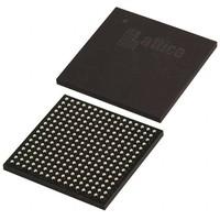
LCMXO2-1200UHC-4FTG256I OverviewThere is a 256-LBGA package that includes this component. FIELD PROGRAMMABLE GATE ARRAY is the component of this type of FPGA. 206 I/Os are available for transferring data more efficiently. A fundamental building block consists of 1280 logic elements/cells. It is powered from a supply voltage of 2.5V. The Surface Mount-slot on the development board allows you to attach the FPGA module. A supply voltage of 2.375V~3.465V is needed in order for fpga chips to operate. As part of the MachXO2 series of FPGAs, it is a type of FPGA. While operating, the operating temperature should be kept within a range of -40°C~100°C TJ. The device has 207 outputs that are integrated into it. As a space-saving measure, this FPGA model is contained within Tray. Total terminations are 256. There are 75776 RAM bits that are available with this device. In order to find related parts, you can use its base part number LCMXO2-1200. There is a maximum RAM si9.3kBe of 9.3kB on this FPGA module, which is necessary to ensure the normal operation of the program. It has a total of 256 pins that are designed for it. 160 LABs and CLBs are built into this FPGA. Providing that this FPGA is mounted in Surface Mount, it will be able to perform according to its specifications in a flawless manner. Designers can fully utilize its flexibility with 2.5V supply voltage. Power is provided by a 2.5/3.3V battery that is included with the device. As far as the pin count is concerned, it has 256 pins. Programs and data can be stored in the 20.5kB memory embedded in this FPGA module. With a frequency of 269MHz, it delivers high efficiency. A 56μA supply current is used for its operation. A CPLD is essentially composed of 640 macrocells, which are the main building blocks of a CPLD. Data is stored in the FLASH memory, so resource conflicts are avoided.
LCMXO2-1200UHC-4FTG256I Features206 I/Os
Up to 75776 RAM bits
256 LABs/CLBs
Operating from a frequency of 269MHz
LCMXO2-1200UHC-4FTG256I ApplicationsThere are a lot of Lattice Semiconductor Corporation
LCMXO2-1200UHC-4FTG256I FPGAs applications.
Device controllers
Software-defined radio
Random logic
ASIC prototyping
Medical imaging
Computer hardware emulation
Integrating multiple SPLDs
Voice recognition
Cryptography
Filtering and communication encoding
| Factory Lead Time | 8 Weeks |
| Mount | Surface Mount |
| Mounting Type | Surface Mount |
| Package / Case | 256-LBGA |
| Number of Pins | 256 |
| Operating Temperature | -40°C~100°C TJ |
| Packaging | Tray |
| Series | MachXO2 |
| Published | 2012 |
| JESD-609 Code | e1 |
| Pbfree Code | yes |
| Part Status | Active |
| Moisture Sensitivity Level (MSL) | 3 (168 Hours) |
| Number of Terminations | 256 |
| ECCN Code | EAR99 |
| Terminal Finish | Tin/Silver/Copper (Sn/Ag/Cu) |
| HTS Code | 8542.39.00.01 |
| Voltage - Supply | 2.375V~3.465V |
| Terminal Position | BOTTOM |
| Terminal Form | BALL |
| Peak Reflow Temperature (Cel) | 260 |
| Supply Voltage | 2.5V |
| Terminal Pitch | 1mm |
| Frequency | 269MHz |
| Time@Peak Reflow Temperature-Max (s) | 30 |
| Base Part Number | LCMXO2-1200 |
| Pin Count | 256 |
| Number of Outputs | 207 |
| Operating Supply Voltage | 2.5V |
| Power Supplies | 2.5/3.3V |
| Memory Size | 20.5kB |
| Operating Supply Current | 56μA |
| Number of I/O | 206 |
| RAM Size | 9.3kB |
| Memory Type | FLASH |
| Propagation Delay | 7.24 ns |
| Programmable Logic Type | FIELD PROGRAMMABLE GATE ARRAY |
| Number of Logic Elements/Cells | 1280 |
| Total RAM Bits | 75776 |
| Number of LABs/CLBs | 160 |
| Number of Macro Cells | 640 |
| REACH SVHC | No SVHC |
| Radiation Hardening | No |
| RoHS Status | ROHS3 Compliant |
| Lead Free | Lead Free |

 LCMXO2-1200UHC-4FTG256I Datasheet
 +8613715157867