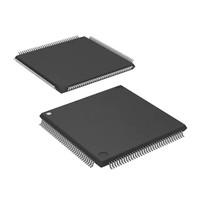
LCMXO2-640UHC-4TG144C OverviewThere are two packages that contain fpga chips: 144-LQFP package and X package. The FIELD PROGRAMMABLE GATE ARRAY-series of FPGAs are composed of this type. Having 107 I/Os makes data transfers more coherent. Logic blocks consist of 640 logic elements/cells. The supply voltage is 2.5V volts. An attachment Surface Mount allows the FPGA module to be attached to the development board. The supply voltage of the device is 2.375V~3.465V , at which it runs. The MachXO2 series FPGA is a type of FPGA that belongs to the MachXO2 family of FPGAs. When operating the machine, it is important to keep the temperature within 0°C~85°C TJ range. This device is equipped with 108 separate outputs, which makes it a very versatile device. There is an FPGA model contained in Tray in order to conserve space. In total, it has 144 terminations on each end. A device like this one offers 65536 RAM bits, which is a considerable amount of memory. In order to find related parts, use the part number LCMXO2-640 as a base. This FPGA module has a RAM si8kBe of 8kB that is sufficient to make sure that the program is able to run normally. In this case, there are 144 pins on the board. A total of 80 LABs/CLBs make up this FPGA array. Having stated that, if this FPGA is mounted in Surface Mount, then it may be able to perform fantastically according to its specifications. The 2.5V supply voltage provides designers with full flexibility in their designs. The device runs on a 2.5/3.3V battery and requires no additional power supply to operate. Data and programs can be stored in this FPGA module's 16.6kB memory. Powered by a 269MHz-frequency motor, it delivers high efficiency. For the building block, it encompasses 640 logic cells that make up the logic circuit. Fpga semiconductor operates on a 3.48mA power supply. As the main building blocks of a CPLD, 320 macro cells make up the majority of the circuit in this device. A FLASH memory provides data storage and avoids resource conflicts.
LCMXO2-640UHC-4TG144C Features107 I/Os
Up to 65536 RAM bits
144 LABs/CLBs
Operating from a frequency of 269MHz
LCMXO2-640UHC-4TG144C ApplicationsThere are a lot of Lattice Semiconductor Corporation
LCMXO2-640UHC-4TG144C FPGAs applications.
Computer hardware emulation
Integrating multiple SPLDs
Voice recognition
Cryptography
Filtering and communication encoding
Aerospace and Defense
Medical Electronics
Audio
Automotive
Consumer Electronics
| Factory Lead Time | 8 Weeks |
| Mount | Surface Mount |
| Mounting Type | Surface Mount |
| Package / Case | 144-LQFP |
| Number of Pins | 144 |
| Operating Temperature | 0°C~85°C TJ |
| Packaging | Tray |
| Series | MachXO2 |
| Published | 2012 |
| JESD-609 Code | e3 |
| Pbfree Code | yes |
| Part Status | Active |
| Moisture Sensitivity Level (MSL) | 3 (168 Hours) |
| Number of Terminations | 144 |
| ECCN Code | EAR99 |
| Terminal Finish | Matte Tin (Sn) |
| HTS Code | 8542.39.00.01 |
| Voltage - Supply | 2.375V~3.465V |
| Terminal Position | QUAD |
| Terminal Form | GULL WING |
| Peak Reflow Temperature (Cel) | 260 |
| Supply Voltage | 2.5V |
| Terminal Pitch | 0.5mm |
| Frequency | 269MHz |
| Time@Peak Reflow Temperature-Max (s) | 30 |
| Base Part Number | LCMXO2-640 |
| Number of Outputs | 108 |
| Qualification Status | Not Qualified |
| Operating Supply Voltage | 2.5V |
| Power Supplies | 2.5/3.3V |
| Memory Size | 16.6kB |
| Operating Supply Current | 3.48mA |
| Number of I/O | 107 |
| RAM Size | 8kB |
| Memory Type | FLASH |
| Propagation Delay | 7.24 ns |
| Programmable Logic Type | FIELD PROGRAMMABLE GATE ARRAY |
| Number of Logic Elements/Cells | 640 |
| Density | 64 kb |
| Total RAM Bits | 65536 |
| Number of LABs/CLBs | 80 |
| Number of Macro Cells | 320 |
| Number of Logic Cells | 640 |
| Length | 20mm |
| Height Seated (Max) | 1.6mm |
| Width | 20mm |
| REACH SVHC | No SVHC |
| RoHS Status | ROHS3 Compliant |
| Lead Free | Lead Free |

 LCMXO2-640UHC-4TG144C Datasheet
 +8613715157867