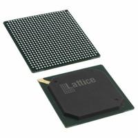
LFE2M50E-5FN672C OverviewThis package is included in the 672-BBGA package and is available for purchase. In this kind of FPGA, FIELD PROGRAMMABLE GATE ARRAY is used. The I/Os are designed to facilitate a more coherent transfer of data. Logic elements/cells form the fundamental building block of a computer. 1.2V volts power it. Using a Surface Mount connector, you can mount this FPGA module on the development board. In order for it to operate, the supply voltage must be 1.14V~1.26V . An FPGA belonging to the ECP2M series is referred to as an FPGA. In order to ensure a safe and efficient operation, it is important to maintain a temperature within 0°C~85°C TJ at all times. With this device, you will be able to make use of 372 outputs. Using the Tray layout, this FPGA model can be contained in a very small amount of space. The total number of terminations is 672. This device is equipped with 4246528 RAM bits in terms of its RAM si4246528e. Parts related to this part can be found using its base part number LFE2M50. During the configuration of this FPGA module, the RAM si518.4kBe reaches 518.4kB to ensure that the program runs normally. The device is designed with 672 pins in total. An array of 6000 LABs/CLBs is built into the FPGA. Fpga electronics is possible for this FPGA to perform as per fpga electronics s specifications as long as fpga electronics is mounted in Surface Mount direction. In the case of 1.2V supply voltage, designers can take full advantage of its flexibility. The device has a total of 672 pins on fpga semiconductor. A crystal oscillating at 311MHz is one of the most common components of this device. Data and programs can be stored in this FPGA module's memory of 531kB. It is composed of 50000 logic cells which serve as the building blocks of the application.
LFE2M50E-5FN672C Features372 I/Os
Up to 4246528 RAM bits
672 LABs/CLBs
LFE2M50E-5FN672C ApplicationsThere are a lot of Lattice Semiconductor Corporation
LFE2M50E-5FN672C FPGAs applications.
ASIC prototyping
Medical imaging
Computer hardware emulation
Integrating multiple SPLDs
Voice recognition
Cryptography
Filtering and communication encoding
Aerospace and Defense
Medical Electronics
Audio
| Factory Lead Time | 8 Weeks |
| Mount | Surface Mount |
| Mounting Type | Surface Mount |
| Package / Case | 672-BBGA |
| Number of Pins | 672 |
| Operating Temperature | 0°C~85°C TJ |
| Packaging | Tray |
| Series | ECP2M |
| Published | 2009 |
| JESD-609 Code | e1 |
| Pbfree Code | yes |
| Part Status | Active |
| Moisture Sensitivity Level (MSL) | 3 (168 Hours) |
| Number of Terminations | 672 |
| ECCN Code | EAR99 |
| Terminal Finish | Tin/Silver/Copper (Sn96.5Ag3.0Cu0.5) |
| HTS Code | 8542.39.00.01 |
| Voltage - Supply | 1.14V~1.26V |
| Terminal Position | BOTTOM |
| Terminal Form | BALL |
| Peak Reflow Temperature (Cel) | 250 |
| Supply Voltage | 1.2V |
| Terminal Pitch | 1mm |
| Reach Compliance Code | not_compliant |
| Time@Peak Reflow Temperature-Max (s) | 30 |
| Base Part Number | LFE2M50 |
| Pin Count | 672 |
| Number of Outputs | 372 |
| Qualification Status | Not Qualified |
| Operating Supply Voltage | 1.2V |
| Memory Size | 531kB |
| Number of I/O | 372 |
| RAM Size | 518.4kB |
| Clock Frequency | 311MHz |
| Programmable Logic Type | FIELD PROGRAMMABLE GATE ARRAY |
| Number of Logic Elements/Cells | 48000 |
| Total RAM Bits | 4246528 |
| Number of LABs/CLBs | 6000 |
| Combinatorial Delay of a CLB-Max | 0.358 ns |
| Number of Logic Cells | 50000 |
| Length | 27mm |
| Height Seated (Max) | 2.6mm |
| Width | 27mm |
| RoHS Status | ROHS3 Compliant |
| Lead Free | Lead Free |

 LFE2M50E-5FN672C Datasheet
 +8613715157867