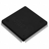
LFXP3C-3QN208C OverviewFpga chips is supplied in the 208-BFQFP package. This kind of FPGA is composed of FIELD PROGRAMMABLE GATE ARRAY. Fpga chips is programmed wFpga chipsh 136 I/Os for transferring data in a more coherent manner. There are 3000 logic elements/cells to form a fundamental building block. Fpga chips is powered from a supply voltage of 1.8V. This FPGA module can be attached to the development board with a Surface Mount. Fpga chips operates wFpga chipsh a supply voltage of 1.71V~3.465V. It is a type of FPGA belonging to the XP seies. The operating temperature should be kept at 0°C~85°C TJ when operating. There are 136 outputs incorporated in this device. This FPGA model is contained in Tray for space saving. Fpga chips is designed wFpga chipsh 208 terminations. The RAM bits that this device offer is 55296. Its base part number LFXP3 can be used to find related parts. The RAM si6.8kBe of this FPGA module reaches 6.8kB to ensure normal operation of the program. Fpga electronics is designed wfpga electronics h 208 pins. As long as this FPGA is mounted in Surface Mount, it could work fantastically according to its specifications. When operating with the supply voltage of 1.8V, designers can fully make use of its flexibility. Fpga electronics operates from a 1.8/2.5/3.3V power supply. Fpga semiconductor is equipped wfpga semiconductorh 208 pin count. This FPGA module embeds a memory of 8.3kB available for storing programs and data. 384 CLBs are basic modules used for its architecture. Fpga semiconductor operates at a frequency of 320MHz to deliver high efficiency. Fpga semiconductor incorporates 384 logic cells used for the building block.
LFXP3C-3QN208C Features136 I/Os
Up to 55296 RAM bits
208 LABs/CLBs
Operating from a frequency of 320MHz
LFXP3C-3QN208C ApplicationsThere are a lot of Lattice Semiconductor Corporation
LFXP3C-3QN208C FPGAs applications.
Digital signal processing
Bioinformatics
Device controllers
Software-defined radio
Random logic
ASIC prototyping
Medical imaging
Computer hardware emulation
Integrating multiple SPLDs
Voice recognition
| Mount | Surface Mount |
| Mounting Type | Surface Mount |
| Package / Case | 208-BFQFP |
| Number of Pins | 208 |
| Operating Temperature | 0°C~85°C TJ |
| Packaging | Tray |
| Series | XP |
| Published | 2000 |
| JESD-609 Code | e3 |
| Pbfree Code | yes |
| Part Status | Obsolete |
| Moisture Sensitivity Level (MSL) | 3 (168 Hours) |
| Number of Terminations | 208 |
| ECCN Code | EAR99 |
| Terminal Finish | Matte Tin (Sn) |
| HTS Code | 8542.39.00.01 |
| Voltage - Supply | 1.71V~3.465V |
| Terminal Position | QUAD |
| Terminal Form | GULL WING |
| Peak Reflow Temperature (Cel) | 245 |
| Supply Voltage | 1.8V |
| Terminal Pitch | 0.5mm |
| Frequency | 320MHz |
| Time@Peak Reflow Temperature-Max (s) | 40 |
| Base Part Number | LFXP3 |
| Pin Count | 208 |
| Number of Outputs | 136 |
| Operating Supply Voltage | 1.8V |
| Power Supplies | 1.8/2.5/3.3V |
| Memory Size | 8.3kB |
| Number of I/O | 136 |
| RAM Size | 6.8kB |
| Organization | 384 CLBS |
| Programmable Logic Type | FIELD PROGRAMMABLE GATE ARRAY |
| Number of Logic Elements/Cells | 3000 |
| Total RAM Bits | 55296 |
| Combinatorial Delay of a CLB-Max | 0.63 ns |
| Number of CLBs | 384 |
| Number of Logic Cells | 384 |
| Length | 28mm |
| Height Seated (Max) | 4.1mm |
| Width | 28mm |
| Radiation Hardening | No |
| RoHS Status | RoHS Compliant |
| Lead Free | Lead Free |

 LFXP3C-3QN208C Datasheet
 +8613715157867