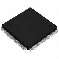
LFXP6C-3QN208C OverviewA 208-BFQFP package contains it, and it is available for download. There are FIELD PROGRAMMABLE GATE ARRAY transistors in this type of FPGA. Its 142 I/Os help it transfer data more efficiently. A fundamental building block contains 6000 logic elements or cells. Power is provided by a 1.8V-volt supply. The Surface Mount-slot connector on the FPGA module can be connected to the development board. Fpga chips operates at a voltage of 1.71V~3.465V and uses a battery to supply power. FPGAs belonging to the XP series are a type of FPGA that belong to the XP series of FPGAs. Operating temperatures should be maintained within the 0°C~85°C TJ range at all times when the unit is in use. During the installation of this device, 142 outputs were incorporated. A model of this FPGA is contained in Tray for the purpose of saving space. In total, there are a total of 208 terminations on fpga chips. Having a RAM bit size of 73728 means that this device will offer you a lot of memory. For related parts, use its base part number LFXP6. A significant amount of RAM is allocated to this FPGA module to ensure that the program can operate normally. This cable has 208 pins and is designed to connect to a computer. Providing the FPGA is mounted in Surface Mount as per the specifications of the IC, then it should work perfectly according to its specifications. With a 1.8V supply voltage, designers can fully utilize the flexibility of the device. Power is supplied to the device by a 1.8/2.5/3.3V battery. Featuring 208 pins in total, it is a versatile device. The basic building block of the system is composed of 750 logic blocks (LABs). In this FPGA module, there is a memory of 11.9kB available for storing applications and data. In order to make the architecture work, 720 CLBs are used. A frequency of 320MHz provides high efficiency. As most of the logic cells for the building blocks are 720 logic cells, it incorporates a lot of logic.
LFXP6C-3QN208C Features142 I/Os
Up to 73728 RAM bits
208 LABs/CLBs
750 logic blocks (LABs)
Operating from a frequency of 320MHz
LFXP6C-3QN208C ApplicationsThere are a lot of Lattice Semiconductor Corporation
LFXP6C-3QN208C FPGAs applications.
Integrating multiple SPLDs
Voice recognition
Cryptography
Filtering and communication encoding
Aerospace and Defense
Medical Electronics
Audio
Automotive
Consumer Electronics
Distributed Monetary Systems
| Mount | Surface Mount |
| Mounting Type | Surface Mount |
| Package / Case | 208-BFQFP |
| Number of Pins | 208 |
| Operating Temperature | 0°C~85°C TJ |
| Packaging | Tray |
| Series | XP |
| Published | 2000 |
| JESD-609 Code | e3 |
| Pbfree Code | yes |
| Part Status | Obsolete |
| Moisture Sensitivity Level (MSL) | 3 (168 Hours) |
| Number of Terminations | 208 |
| ECCN Code | EAR99 |
| Terminal Finish | Matte Tin (Sn) |
| HTS Code | 8542.39.00.01 |
| Voltage - Supply | 1.71V~3.465V |
| Terminal Position | QUAD |
| Terminal Form | GULL WING |
| Peak Reflow Temperature (Cel) | 245 |
| Supply Voltage | 1.8V |
| Terminal Pitch | 0.5mm |
| Reach Compliance Code | unknown |
| Frequency | 320MHz |
| Time@Peak Reflow Temperature-Max (s) | 40 |
| Base Part Number | LFXP6 |
| Pin Count | 208 |
| Number of Outputs | 142 |
| Qualification Status | Not Qualified |
| Operating Supply Voltage | 1.8V |
| Power Supplies | 1.8/2.5/3.3V |
| Memory Size | 11.9kB |
| Number of I/O | 142 |
| RAM Size | 9kB |
| Organization | 720 CLBS |
| Programmable Logic Type | FIELD PROGRAMMABLE GATE ARRAY |
| Number of Logic Elements/Cells | 6000 |
| Total RAM Bits | 73728 |
| Number of Logic Blocks (LABs) | 750 |
| Combinatorial Delay of a CLB-Max | 0.63 ns |
| Number of CLBs | 720 |
| Number of Logic Cells | 720 |
| Length | 28mm |
| Height Seated (Max) | 4.1mm |
| Width | 28mm |
| RoHS Status | RoHS Compliant |
| Lead Free | Lead Free |
