PCK2002PD,118 OverviewThe clock divider is available in 8-SOIC (0.154, 3.90mm Width) case. There is a Tape & Reel (TR) package attached to it. It is normal to operate with a value of 533MHz. A total of 8 terminations are present. Supply voltages of 3.3V enable high efficiency. As you can see, it is mounted by Surface Mount. An electronic component classified as Fanout Buffer (Distribution) is categorized as such. Set the temperature to -40°C~85°C for reliable performance. The clock switch should be able to be powered by a 3V~3.6V V source. There is a pin count of 8 on timeing clock. This object belongs to the PCK2002 family. There is 3.6V maximum supply voltage (Vsup). The supply voltage (Vsup) should be maintained above 3V in order for the clock divider to operate normally. A 3.3V volt supply powers it. It is possible to obtain 4 true outputs.
PCK2002PD,118 Features8 terminations
The operating temperature of -40°C~85°C degrees
PCK2002PD,118 ApplicationsThere are a lot of NXP USA Inc.
PCK2002PD,118 Clock Buffers & Drivers applications.
Machine made
Clock signal duplication
Clock signal format conversion
Clock signal level shifting
High performance communication system
Data center
Cloud computing
Network
High speed industry
High-end consumer electronics
| Mounting Type | Surface Mount |
| Package / Case | 8-SOIC (0.154, 3.90mm Width) |
| Surface Mount | YES |
| Operating Temperature | -40°C~85°C |
| Packaging | Tape & Reel (TR) |
| Published | 2002 |
| JESD-609 Code | e4 |
| Part Status | Obsolete |
| Moisture Sensitivity Level (MSL) | 1 (Unlimited) |
| Number of Terminations | 8 |
| Type | Fanout Buffer (Distribution) |
| Terminal Finish | NICKEL PALLADIUM GOLD |
| Voltage - Supply | 3V~3.6V |
| Terminal Position | DUAL |
| Terminal Form | GULL WING |
| Peak Reflow Temperature (Cel) | 260 |
| Number of Functions | 1 |
| Supply Voltage | 3.3V |
| Time@Peak Reflow Temperature-Max (s) | 40 |
| Base Part Number | PCK2002 |
| Pin Count | 8 |
| JESD-30 Code | R-PDSO-G8 |
| Qualification Status | Not Qualified |
| Supply Voltage-Max (Vsup) | 3.6V |
| Power Supplies | 3.3V |
| Supply Voltage-Min (Vsup) | 3V |
| Number of Circuits | 1 |
| Frequency (Max) | 533MHz |
| Input | LVTTL |
| Ratio - Input:Output | 1:4 |
| Max I(ol) | 0.024 A |
| Differential - Input:Output | No/No |
| Prop. Delay@Nom-Sup | 3.4 ns |
| Propagation Delay (tpd) | 3.4 ns |
| fmax-Min | 533 MHz |
| Same Edge Skew-Max (tskwd) | 0.2 ns |
| Number of True Outputs | 4 |
| Length | 4.9mm |
| Width | 3.9mm |
| RoHS Status | ROHS3 Compliant |
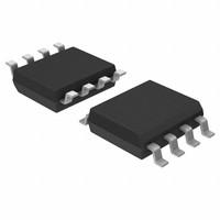

 PCK2002PD,118 Datasheet
 +8613715157867