XC2V250-4FGG256C OverviewThe package that contains this software is called 256-BGA. A FIELD PROGRAMMABLE GATE ARRAY-based FPGA is one of these types. There are 172 I/Os for better data transfer. In order for the device to operate, a supply voltage of 1.5V volts needs to be provided. FPGA modules can be attached to development boards using a Surface Mount-connector. This device is powered by a 1.425V~1.575V battery. There are many types of FPGAs in the Virtex®-II series, this is one of them. Fpga chips is recommended that the operating temperature be kept wFpga chipshin the range 0°C~85°C TJ while the machine is operating. A device such as this one has 172 outputs built into it. Fpga chips is designed to maximiTraye space efficiency by containing the FPGA model in Tray. In total, it has a total of 256 terminations. As far as the RAM bits are concerned, this device offers you a total of 442368. If you are looking for related parts, you can use the base part number XC2V250 as a starting point. For the program to work properly, the RAM si54kBe of this FPGA module must reach 54kB GB in order to ensure normal operation. In this case, 256 pins are used in the design. 384 LABs/CLBs are configured on this FPGA. In my opinion, this FPGA could produce fantastic results if mounted in Surface Mount, provided that its specifications are followed. Design engineers can fully take advantage of its flexibility when operating at 1.5V supply voltage. In order for fpga electronics to work, fpga electronics requires a 1.51.5/3.33.3V power supply. As a basic building block, fpga semiconductor consists of 250000 gates. A total of 256 pins are included in this device. Most of the time, it uses a crystal oscillating at 650MHz to generate the signal. In order to store and transfer data, a total of 3072 registers are used. An architecture consists of 384 CLBs.
XC2V250-4FGG256C Features172 I/Os
Up to 442368 RAM bits
256 LABs/CLBs
3072 registers
XC2V250-4FGG256C ApplicationsThere are a lot of Xilinx Inc.
XC2V250-4FGG256C FPGAs applications.
Random logic
ASIC prototyping
Medical imaging
Computer hardware emulation
Integrating multiple SPLDs
Voice recognition
Cryptography
Filtering and communication encoding
Aerospace and Defense
Medical Electronics
| Mount | Surface Mount |
| Mounting Type | Surface Mount |
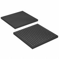
| Package / Case | 256-BGA |
| Number of Pins | 256 |
| Operating Temperature | 0°C~85°C TJ |
| Packaging | Tray |
| Series | Virtex®-II |
| Published | 2007 |
| JESD-609 Code | e1 |
| Pbfree Code | yes |
| Part Status | Obsolete |
| Moisture Sensitivity Level (MSL) | 3 (168 Hours) |
| Number of Terminations | 256 |
| ECCN Code | EAR99 |
| Voltage - Supply | 1.425V~1.575V |
| Terminal Position | BOTTOM |
| Terminal Form | BALL |
| Peak Reflow Temperature (Cel) | 260 |
| Supply Voltage | 1.5V |
| Terminal Pitch | 1mm |
| Time@Peak Reflow Temperature-Max (s) | 30 |
| Base Part Number | XC2V250 |
| Pin Count | 256 |
| Number of Outputs | 172 |
| Operating Supply Voltage | 1.5V |
| Power Supplies | 1.51.5/3.33.3V |
| Number of I/O | 172 |
| RAM Size | 54kB |
| Clock Frequency | 650MHz |
| Programmable Logic Type | FIELD PROGRAMMABLE GATE ARRAY |
| Total RAM Bits | 442368 |
| Number of Gates | 250000 |
| Number of LABs/CLBs | 384 |
| Speed Grade | 4 |
| Number of Registers | 3072 |
| Number of CLBs | 384 |
| Length | 17mm |
| Height Seated (Max) | 2mm |
| Width | 17mm |
| Radiation Hardening | No |
| RoHS Status | RoHS Compliant |
| Lead Free | Lead Free |

 XC2V250-4FGG256C Datasheet
 +8613715157867