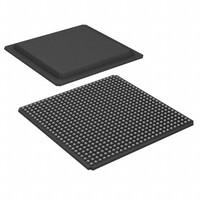
XC2VP40-5FG676C OverviewA 676-BBGA, FCBGA package is provided with this component. FPGAs of this type consist of FIELD PROGRAMMABLE GATE ARRAY components. This device features 416 I/Os in order to transfer data in a more efficient manner. A fundamental building block is made up of 43632 logic elements/cells. An electrical supply voltage of 1.5V powers it. An FPGA module can be attached to a development board with a Surface Mount-pin. Powered by a 1.425V~1.575V supply voltage, fpga chips is able to operate at high speeds. The FPGA belongs to the Virtex®-II Pro series of FPGAs, and it is one type of FPGA. During the operation of the system, the operating temperature should remain within the range of 0°C~85°C TJ. In order to make this device as versatile as possible, there are 416 different outputs included. It is for space saving reasons that this FPGA model is contained in Bulk. As a whole, it has 676 terminations. The RAM bits that are offered by this fpga chips are 3538944. The FPGA module's RAM si432kBe reaches 432kB in order to ensure that the program operates in a normal manner. Fpga electronics contains 4848 LABs/CLBs in an array. A 1.5V-volt supply allows designers to fully utilize its flexibility. In addition to this, it has 676 pins. As a result, there are 38784 registers which are used to store and transfer data.
XC2VP40-5FG676C Features416 I/Os
Up to 3538944 RAM bits
38784 registers
XC2VP40-5FG676C ApplicationsThere are a lot of Xilinx Inc.
XC2VP40-5FG676C FPGAs applications.
Medical imaging
Computer hardware emulation
Integrating multiple SPLDs
Voice recognition
Cryptography
Filtering and communication encoding
Aerospace and Defense
Medical Electronics
Audio
Automotive
| Factory Lead Time | 6 Weeks |
| Mounting Type | Surface Mount |
| Package / Case | 676-BBGA, FCBGA |
| Surface Mount | YES |
| Operating Temperature | 0°C~85°C TJ |
| Packaging | Bulk |
| Series | Virtex®-II Pro |
| Published | 2011 |
| JESD-609 Code | e0 |
| Pbfree Code | no |
| Part Status | Obsolete |
| Moisture Sensitivity Level (MSL) | 2A (4 Weeks) |
| Number of Terminations | 676 |
| ECCN Code | 3A991.D |
| Terminal Finish | Tin/Lead (Sn63Pb37) |
| Voltage - Supply | 1.425V~1.575V |
| Terminal Position | BOTTOM |
| Terminal Form | BALL |
| Peak Reflow Temperature (Cel) | 225 |
| Supply Voltage | 1.5V |
| Terminal Pitch | 1mm |
| Reach Compliance Code | not_compliant |
| Time@Peak Reflow Temperature-Max (s) | 30 |
| Pin Count | 676 |
| JESD-30 Code | S-PBGA-B676 |
| Number of Outputs | 416 |
| Qualification Status | Not Qualified |
| Operating Supply Voltage | 1.5V |
| Number of I/O | 416 |
| RAM Size | 432kB |
| Number of Inputs | 416 |
| Programmable Logic Type | FIELD PROGRAMMABLE GATE ARRAY |
| Number of Logic Elements/Cells | 43632 |
| Total RAM Bits | 3538944 |
| Number of LABs/CLBs | 4848 |
| Speed Grade | 5 |
| Number of Registers | 38784 |
| Combinatorial Delay of a CLB-Max | 0.36 ns |
| Length | 27mm |
| Height Seated (Max) | 2.44mm |
| Width | 27mm |
| RoHS Status | Non-RoHS Compliant |
