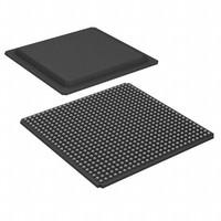
XC3S2000-5FG676C OverviewAs part of the 676-BBGA, FCBGA package, it is included. This kind of FPGA is composed of FIELD PROGRAMMABLE GATE ARRAY. A total of 489 I/Os allow data to be transferred in a more coherent manner. A fundamental building block consists of 46080 logic elements/cells. It is powered from a supply voltage of 1.2V. With a Surface Mount connector, this FPGA module can be attached to the development board. In order to operate it, it requires a voltage supply of 1.14V~1.26V . It is a type of FPGA that belongs to the Spartan®-3 series of FPGAs. Fpga chips is important to maintain the operating temperature wFpga chipshin the range of 0°C~85°C TJ when operating the machine. In this device, there are 489 outputs that can be used. In order to save space, this FPGA model has been contained in Bulk. There are a total of 676 terminations. This device has 737280 RAM bits, which is the number of RAM bits that this device offers. Fpga electronics is important that this FPGA module has a RAM si90kBe of 90kB in order to ensure that the program will run normally. The FPGA consists of 5120 LABs/CLBs. Its flexibility can be fully utilized when operating with a 1.2V supply voltage. The basic building block of this system consists of 2000000 gates. There are a total of 676 pins on this device.
XC3S2000-5FG676C Features489 I/Os
Up to 737280 RAM bits
XC3S2000-5FG676C ApplicationsThere are a lot of Xilinx Inc.
XC3S2000-5FG676C FPGAs applications.
Bioinformatics
Device controllers
Software-defined radio
Random logic
ASIC prototyping
Medical imaging
Computer hardware emulation
Integrating multiple SPLDs
Voice recognition
Cryptography
| Factory Lead Time | 10 Weeks |
| Mounting Type | Surface Mount |
| Package / Case | 676-BBGA, FCBGA |
| Surface Mount | YES |
| Operating Temperature | 0°C~85°C TJ |
| Packaging | Bulk |
| Series | Spartan®-3 |
| Published | 2009 |
| JESD-609 Code | e0 |
| Pbfree Code | no |
| Part Status | Active |
| Moisture Sensitivity Level (MSL) | 3 (168 Hours) |
| Number of Terminations | 676 |
| ECCN Code | 3A991.D |
| Terminal Finish | Tin/Lead (Sn63Pb37) |
| Voltage - Supply | 1.14V~1.26V |
| Terminal Position | BOTTOM |
| Terminal Form | BALL |
| Peak Reflow Temperature (Cel) | 225 |
| Supply Voltage | 1.2V |
| Terminal Pitch | 1mm |
| Reach Compliance Code | not_compliant |
| Time@Peak Reflow Temperature-Max (s) | 30 |
| Pin Count | 676 |
| JESD-30 Code | S-PBGA-B676 |
| Number of Outputs | 489 |
| Qualification Status | Not Qualified |
| Operating Supply Voltage | 1.2V |
| Number of I/O | 489 |
| RAM Size | 90kB |
| Number of Inputs | 489 |
| Programmable Logic Type | FIELD PROGRAMMABLE GATE ARRAY |
| Number of Logic Elements/Cells | 46080 |
| Total RAM Bits | 737280 |
| Number of Gates | 2000000 |
| Number of LABs/CLBs | 5120 |
| Speed Grade | 5 |
| Length | 27mm |
| Height Seated (Max) | 2.6mm |
| Width | 27mm |
| RoHS Status | Non-RoHS Compliant |

 XC3S2000-5FG676C Datasheet
 +8613715157867