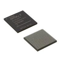
Products DetailsXC7A50T-2CSG324I Overview
In the package 324-LFBGA, CSPBGA, this product is provided. Fpga chips consists of FIELD PROGRAMMABLE GATE ARRAY elements. A total of 210 I/Os are programmed to ensure a more coherent data transfer. The basic building blocks of logic contain 52160 logic elements/cells. Supply voltage is 1V volts. By attaching the Surface Mount connector, you can use this FPGA module with your development board. With a supply voltage of 0.95V~1.05V, this device operates with ease. This is a type of FPGA that is part of the Artix-7 series of FPGAs. Fpga chips is necessary to keep the operating temperature wFpga chipshin -40°C~100°C TJ when the device is operating. In this device, 210 outputs are incorporated in order to provide you with maximum flexibility. As a result of space limitations, this FPGA model has been included in Tray. In total, the terminations of this piece are 324. Fpga electronics is worth mentioning that this device provides 2764800 bfpga electronics s of RAM. The RAM si337.5kBe of this FPGA module reaches 337.5kB so as to guarantee the normal operation of the program during operation. The device has 325 pins which are included in the design. The FPGA is built as an array of 4075 latches or CLBs. I think, as long as this FPGA is mounted in Surface Mount, it could perform excellently according to its specifications as long as you mount it in Surface Mount. This is a battery operated device that operates on 1V. I am going to present you with a device that is equipped with 324 pins. The structure of the registers used to store and transfer data consists of 65200 registers.
XC7A50T-2CSG324I Features
210 I/Os
Up to 2764800 RAM bits
325 LABs/CLBs
65200 registers
XC7A50T-2CSG324I Applications
There are a lot of Xilinx Inc.
XC7A50T-2CSG324I FPGAs applications.
Voice recognition
Cryptography
Filtering and communication encoding
Aerospace and Defense
Medical Electronics
Audio
Automotive
Consumer Electronics
Distributed Monetary Systems
Data Center

 XC7A50T-2CSG324I Datasheet
 +8613715157867