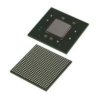
XC7K160T-1FBG484I OverviewThe package that contains this software is called 484-BBGA, FCBGA. A FIELD PROGRAMMABLE GATE ARRAY-based FPGA is one of these types. There are 285 I/Os for better data transfer. In order to construct a fundamental building block, 162240 logic elements/cells are required. In order for the device to operate, a supply voltage of 1V volts needs to be provided. FPGA modules can be attached to development boards using a Surface Mount-connector. This device is powered by a 0.97V~1.03V battery. There are many types of FPGAs in the Kintex®-7 series, this is one of them. Fpga chips is recommended that the operating temperature be kept wFpga chipshin the range -40°C~100°C TJ while the machine is operating. A device such as this one has 285 outputs built into it. Fpga chips is designed to maximiTraye space efficiency by containing the FPGA model in Tray. In total, it has a total of 484 terminations. As far as the RAM bits are concerned, this device offers you a total of 11980800. If you are looking for related parts, you can use the base part number XC7K160 as a starting point. For the program to work properly, the RAM si1.4MBe of this FPGA module must reach 1.4MB GB in order to ensure normal operation. 12675 LABs/CLBs are configured on this FPGA. In order for fpga electronics to work, fpga electronics requires a 11.83.3V power supply. A total of 484 pins are included in this device. Most of the time, it uses a crystal oscillating at 1098MHz to generate the signal. In order to store and transfer data, a total of 202800 registers are used.
XC7K160T-1FBG484I Features285 I/Os
Up to 11980800 RAM bits
202800 registers
XC7K160T-1FBG484I ApplicationsThere are a lot of Xilinx Inc.
XC7K160T-1FBG484I FPGAs applications.
Random logic
ASIC prototyping
Medical imaging
Computer hardware emulation
Integrating multiple SPLDs
Voice recognition
Cryptography
Filtering and communication encoding
Aerospace and Defense
Medical Electronics
| Factory Lead Time | 10 Weeks |
| Contact Plating | Copper, Silver, Tin |
| Mounting Type | Surface Mount |
| Package / Case | 484-BBGA, FCBGA |
| Surface Mount | YES |
| Operating Temperature | -40°C~100°C TJ |
| Packaging | Tray |
| Series | Kintex®-7 |
| Published | 2010 |
| JESD-609 Code | e1 |
| Pbfree Code | yes |
| Part Status | Active |
| Moisture Sensitivity Level (MSL) | 4 (72 Hours) |
| Number of Terminations | 484 |
| ECCN Code | 3A991.D |
| Terminal Finish | Tin/Silver/Copper (Sn96.5Ag3.0Cu0.5) |
| HTS Code | 8542.39.00.01 |
| Voltage - Supply | 0.97V~1.03V |
| Terminal Position | BOTTOM |
| Terminal Form | BALL |
| Supply Voltage | 1V |
| Terminal Pitch | 1mm |
| Base Part Number | XC7K160 |
| Pin Count | 484 |
| JESD-30 Code | S-PBGA-B484 |
| Number of Outputs | 285 |
| Power Supplies | 11.83.3V |
| Number of I/O | 285 |
| RAM Size | 1.4MB |
| Clock Frequency | 1098MHz |
| Propagation Delay | 120 ps |
| Number of Inputs | 285 |
| Programmable Logic Type | FIELD PROGRAMMABLE GATE ARRAY |
| Number of Logic Elements/Cells | 162240 |
| Total RAM Bits | 11980800 |
| Number of LABs/CLBs | 12675 |
| Speed Grade | -1 |
| Number of Registers | 202800 |
| Combinatorial Delay of a CLB-Max | 0.74 ns |
| Length | 23mm |
| Height Seated (Max) | 2.54mm |
| Width | 23mm |
| Radiation Hardening | No |
| RoHS Status | ROHS3 Compliant |

 XC7K160T-1FBG484I Datasheet
 +8613715157867