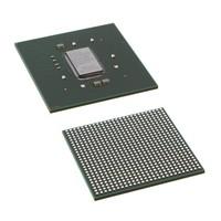
XC7K325T-1FFG676I OverviewFpga chips is supplied in the 676-BBGA, FCBGA package. This kind of FPGA is composed of FIELD PROGRAMMABLE GATE ARRAY. Fpga chips is programmed wFpga chipsh 400 I/Os for transferring data in a more coherent manner. There are 326080 logic elements/cells to form a fundamental building block. Fpga chips is powered from a supply voltage of 1V. This FPGA module can be attached to the development board with a Surface Mount. Fpga chips operates wFpga chipsh a supply voltage of 0.97V~1.03V. It is a type of FPGA belonging to the Kintex®-7 seies. The operating temperature should be kept at -40°C~100°C TJ when operating. There are 400 outputs incorporated in this device. This FPGA model is contained in Tray for space saving. Fpga chips is designed wFpga chipsh 676 terminations. The RAM bits that this device offer is 16404480. Its base part number XC7K325T can be used to find related parts. The RAM si2MBe of this FPGA module reaches 2MB to ensure normal operation of the program. This FPGA is built as an array of 25475 LABs/CLBs. Fpga electronics operates from a 11.83.3V power supply. Fpga semiconductor is equipped wfpga semiconductorh 676 pin count. Typically, fpga semiconductor uses a crystal oscillating at 1098MHz . This FPGA module embeds a memory of 1GB available for storing programs and data. There are 407600 registers used to store and transfer data. The DDR3 memory is adopted for storing data and avoiding resource conflicts.
XC7K325T-1FFG676I Features400 I/Os
Up to 16404480 RAM bits
407600 registers
XC7K325T-1FFG676I ApplicationsThere are a lot of Xilinx Inc.
XC7K325T-1FFG676I FPGAs applications.
Digital signal processing
Bioinformatics
Device controllers
Software-defined radio
Random logic
ASIC prototyping
Medical imaging
Computer hardware emulation
Integrating multiple SPLDs
Voice recognition
| Factory Lead Time | 11 Weeks |
| Mounting Type | Surface Mount |
| Package / Case | 676-BBGA, FCBGA |
| Surface Mount | YES |
| Operating Temperature | -40°C~100°C TJ |
| Packaging | Tray |
| Series | Kintex®-7 |
| Published | 2009 |
| JESD-609 Code | e1 |
| Pbfree Code | yes |
| Part Status | Active |
| Moisture Sensitivity Level (MSL) | 4 (72 Hours) |
| Number of Terminations | 676 |
| ECCN Code | 3A991.D |
| Terminal Finish | Tin/Silver/Copper (Sn96.5Ag3.0Cu0.5) |
| HTS Code | 8542.39.00.01 |
| Voltage - Supply | 0.97V~1.03V |
| Terminal Position | BOTTOM |
| Terminal Form | BALL |
| Peak Reflow Temperature (Cel) | NOT SPECIFIED |
| Supply Voltage | 1V |
| Terminal Pitch | 1mm |
| Reach Compliance Code | not_compliant |
| Time@Peak Reflow Temperature-Max (s) | NOT SPECIFIED |
| Base Part Number | XC7K325T |
| Pin Count | 676 |
| JESD-30 Code | S-PBGA-B676 |
| Number of Outputs | 400 |
| Qualification Status | Not Qualified |
| Power Supplies | 11.83.3V |
| Memory Size | 1GB |
| Number of I/O | 400 |
| RAM Size | 2MB |
| Memory Type | DDR3 |
| Clock Frequency | 1098MHz |
| Number of Inputs | 400 |
| Programmable Logic Type | FIELD PROGRAMMABLE GATE ARRAY |
| Number of Logic Elements/Cells | 326080 |
| Total RAM Bits | 16404480 |
| Number of LABs/CLBs | 25475 |
| Speed Grade | -1 |
| Number of Registers | 407600 |
| Combinatorial Delay of a CLB-Max | 0.74 ns |
| Length | 27mm |
| Height Seated (Max) | 3.37mm |
| Width | 27mm |
| RoHS Status | ROHS3 Compliant |

 XC7K325T-1FFG676I Datasheet
 +8613715157867