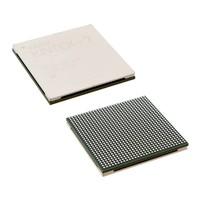
XC7K325T-L2FFG900E OverviewThe package that contains this software is called 900-BBGA, FCBGA. A FIELD PROGRAMMABLE GATE ARRAY-based FPGA is one of these types. There are 500 I/Os for better data transfer. In order to construct a fundamental building block, 326080 logic elements/cells are required. In order for the device to operate, a supply voltage of 0.9V volts needs to be provided. FPGA modules can be attached to development boards using a Surface Mount-connector. This device is powered by a 0.87V~0.93V battery. There are many types of FPGAs in the Kintex®-7 series, this is one of them. Fpga chips is recommended that the operating temperature be kept wFpga chipshin the range 0°C~100°C TJ while the machine is operating. A device such as this one has 500 outputs built into it. Fpga chips is designed to maximiTraye space efficiency by containing the FPGA model in Tray. In total, it has a total of 900 terminations. As far as the RAM bits are concerned, this device offers you a total of 16404480. If you are looking for related parts, you can use the base part number XC7K325T as a starting point. For the program to work properly, the RAM si2MBe of this FPGA module must reach 2MB GB in order to ensure normal operation. 25475 LABs/CLBs are configured on this FPGA. In my opinion, this FPGA could produce fantastic results if mounted in Surface Mount, provided that its specifications are followed. In order for fpga electronics to work, fpga electronics requires a 0.91.83.3V power supply. A total of 900 pins are included in this device. In this FPGA module, there is a memory of 1GB that can be used to store programs and data. In order to store and transfer data, a total of 407600 registers are used. Furthermore, it can be distinguished by the presence of a feature called ALSO OPERATES AT 1 V SUPPLY. This memory is designed for storing data and avoiding resource conflicts.
XC7K325T-L2FFG900E Features500 I/Os
Up to 16404480 RAM bits
407600 registers
XC7K325T-L2FFG900E ApplicationsThere are a lot of Xilinx Inc.
XC7K325T-L2FFG900E FPGAs applications.
Random logic
ASIC prototyping
Medical imaging
Computer hardware emulation
Integrating multiple SPLDs
Voice recognition
Cryptography
Filtering and communication encoding
Aerospace and Defense
Medical Electronics
| Factory Lead Time | 11 Weeks |
| Mount | Surface Mount |
| Mounting Type | Surface Mount |
| Package / Case | 900-BBGA, FCBGA |
| Operating Temperature | 0°C~100°C TJ |
| Packaging | Tray |
| Series | Kintex®-7 |
| Published | 2009 |
| JESD-609 Code | e1 |
| Pbfree Code | yes |
| Part Status | Active |
| Moisture Sensitivity Level (MSL) | 4 (72 Hours) |
| Number of Terminations | 900 |
| ECCN Code | 3A991.D |
| Terminal Finish | Tin/Silver/Copper (Sn96.5Ag3.0Cu0.5) |
| Additional Feature | ALSO OPERATES AT 1 V SUPPLY |
| HTS Code | 8542.39.00.01 |
| Voltage - Supply | 0.87V~0.93V |
| Terminal Position | BOTTOM |
| Terminal Form | BALL |
| Peak Reflow Temperature (Cel) | NOT SPECIFIED |
| Supply Voltage | 0.9V |
| Terminal Pitch | 1mm |
| Reach Compliance Code | not_compliant |
| Time@Peak Reflow Temperature-Max (s) | NOT SPECIFIED |
| Base Part Number | XC7K325T |
| Pin Count | 900 |
| JESD-30 Code | S-PBGA-B900 |
| Number of Outputs | 500 |
| Qualification Status | Not Qualified |
| Power Supplies | 0.91.83.3V |
| Memory Size | 1GB |
| Number of I/O | 500 |
| RAM Size | 2MB |
| Memory Type | DDR3 |
| Number of Inputs | 500 |
| Programmable Logic Type | FIELD PROGRAMMABLE GATE ARRAY |
| Number of Logic Elements/Cells | 326080 |
| Total RAM Bits | 16404480 |
| Number of LABs/CLBs | 25475 |
| Number of Registers | 407600 |
| Combinatorial Delay of a CLB-Max | 0.91 ns |
| Length | 31mm |
| Height Seated (Max) | 3.35mm |
| Width | 31mm |
| RoHS Status | ROHS3 Compliant |

 XC7K325T-L2FFG900E Datasheet
 +8613715157867