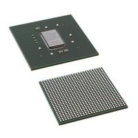
XC7K410T-L2FFG676I OverviewIn the 676-BBGA, FCBGA package, you will find fpga chips. An FPGA of this type is made up of FIELD PROGRAMMABLE GATE ARRAY gates. The device has 400 I/O ports for more coherent data transfer. To form a fundamental building block, there are 406720 logic elements/cells. In order to operate fpga chips, a voltage supply of 0.95V volts is required. Surface Mount-connectors can be used to attach this FPGA module to the development board. There is a 0.97V~1.03V-volt supply voltage required for the device to operate. The Kintex®-7 Series is one of the types of FPGAs that belong to this type. As far as the operating temperature is concerned, it should be kept within -40°C~100°C TJ when operating. Unlike other FPGA models, this one is contained in Tray for the sake of space saving. 676 terminations are present in total. Fpga chips is important to note that this device has a RAM capacFpga chipsy of 29306880 bFpga chipss. It is crucial that the RAM si3.5MBe of this FPGA module reaches 3.5MB so that the program can run normally. A total of 31775 LABs/CLBs are included in this FPGA. In order for this FPGA to work properly in accordance with its specifications, it is necessary that it is mounted in Surface Mount.
XC7K410T-L2FFG676I Features400 I/Os
Up to 29306880 RAM bits
XC7K410T-L2FFG676I ApplicationsThere are a lot of Xilinx Inc.
XC7K410T-L2FFG676I FPGAs applications.
Software-defined radio
Random logic
ASIC prototyping
Medical imaging
Computer hardware emulation
Integrating multiple SPLDs
Voice recognition
Cryptography
Filtering and communication encoding
Aerospace and Defense
| Factory Lead Time | 12 Weeks |
| Mount | Surface Mount |
| Mounting Type | Surface Mount |
| Package / Case | 676-BBGA, FCBGA |
| Operating Temperature | -40°C~100°C TJ |
| Packaging | Tray |
| Series | Kintex®-7 |
| Published | 2010 |
| JESD-609 Code | e1 |
| Part Status | Active |
| Moisture Sensitivity Level (MSL) | 4 (72 Hours) |
| Number of Terminations | 676 |
| ECCN Code | 3A991.D |
| Terminal Finish | Tin/Silver/Copper (Sn/Ag/Cu) |
| HTS Code | 8542.39.00.01 |
| Voltage - Supply | 0.97V~1.03V |
| Terminal Position | BOTTOM |
| Terminal Form | BALL |
| Peak Reflow Temperature (Cel) | NOT SPECIFIED |
| Supply Voltage | 0.95V |
| Terminal Pitch | 1mm |
| Reach Compliance Code | not_compliant |
| Time@Peak Reflow Temperature-Max (s) | NOT SPECIFIED |
| JESD-30 Code | S-PBGA-B676 |
| Number of I/O | 400 |
| RAM Size | 3.5MB |
| Programmable Logic Type | FIELD PROGRAMMABLE GATE ARRAY |
| Number of Logic Elements/Cells | 406720 |
| Total RAM Bits | 29306880 |
| Number of LABs/CLBs | 31775 |
| Combinatorial Delay of a CLB-Max | 0.61 ns |
| Length | 27mm |
| Height Seated (Max) | 3.37mm |
| Width | 27mm |
| RoHS Status | ROHS3 Compliant |

 XC7K410T-L2FFG676I Datasheet
 +8613715157867