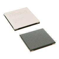
XC7K480T-2FFG901I OverviewIn the package 900-BBGA, FCBGA, this product is provided. Fpga chips consists of FIELD PROGRAMMABLE GATE ARRAY elements. A total of 380 I/Os are programmed to ensure a more coherent data transfer. The basic building blocks of logic contain 477760 logic elements/cells. Supply voltage is 1V volts. By attaching the Surface Mount connector, you can use this FPGA module with your development board. With a supply voltage of 0.97V~1.03V, this device operates with ease. This is a type of FPGA that is part of the Kintex®-7 series of FPGAs. Fpga chips is necessary to keep the operating temperature wFpga chipshin -40°C~100°C TJ when the device is operating. In this device, 380 outputs are incorporated in order to provide you with maximum flexibility. As a result of space limitations, this FPGA model has been included in Tray. In total, the terminations of this piece are 901. Fpga electronics is worth mentioning that this device provides 35205120 bfpga electronics s of RAM. XC7K480 is the base part number that can be used to identify related parts. The RAM si4.2MBe of this FPGA module reaches 4.2MB so as to guarantee the normal operation of the program during operation. The FPGA is built as an array of 37325 latches or CLBs. This is a battery operated device that operates on 11.83.3V. I am going to present you with a device that is equipped with 901 pins. Fpga semiconductor typically uses a crystal oscillating at 1286MHz. The structure of the registers used to store and transfer data consists of 597200 registers.
XC7K480T-2FFG901I Features380 I/Os
Up to 35205120 RAM bits
597200 registers
XC7K480T-2FFG901I ApplicationsThere are a lot of Xilinx Inc.
XC7K480T-2FFG901I FPGAs applications.
Voice recognition
Cryptography
Filtering and communication encoding
Aerospace and Defense
Medical Electronics
Audio
Automotive
Consumer Electronics
Distributed Monetary Systems
Data Center
| Factory Lead Time | 10 Weeks |
| Mounting Type | Surface Mount |
| Package / Case | 900-BBGA, FCBGA |
| Surface Mount | YES |
| Operating Temperature | -40°C~100°C TJ |
| Packaging | Tray |
| Series | Kintex®-7 |
| Published | 2010 |
| JESD-609 Code | e1 |
| Pbfree Code | yes |
| Part Status | Active |
| Moisture Sensitivity Level (MSL) | 4 (72 Hours) |
| Number of Terminations | 901 |
| ECCN Code | 3A991.D |
| Terminal Finish | Tin/Silver/Copper (Sn/Ag/Cu) |
| HTS Code | 8542.39.00.01 |
| Voltage - Supply | 0.97V~1.03V |
| Terminal Position | BOTTOM |
| Terminal Form | BALL |
| Supply Voltage | 1V |
| Terminal Pitch | 1mm |
| Base Part Number | XC7K480 |
| Pin Count | 901 |
| JESD-30 Code | S-PBGA-B901 |
| Number of Outputs | 380 |
| Power Supplies | 11.83.3V |
| Number of I/O | 380 |
| RAM Size | 4.2MB |
| Clock Frequency | 1286MHz |
| Number of Inputs | 380 |
| Programmable Logic Type | FIELD PROGRAMMABLE GATE ARRAY |
| Number of Logic Elements/Cells | 477760 |
| Total RAM Bits | 35205120 |
| Number of LABs/CLBs | 37325 |
| Speed Grade | -2 |
| Number of Registers | 597200 |
| Combinatorial Delay of a CLB-Max | 0.61 ns |
| Length | 31mm |
| Height Seated (Max) | 3.35mm |
| Width | 31mm |
| Radiation Hardening | No |
| RoHS Status | ROHS3 Compliant |

 XC7K480T-2FFG901I Datasheet
 +8613715157867