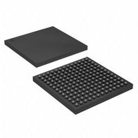
10M08SAU169I7G OverviewThe package that contains this software is called 169-LFBGA. A FIELD PROGRAMMABLE GATE ARRAY-based FPGA is one of these types. There are 130 I/Os for better data transfer. In order to construct a fundamental building block, 8000 logic elements/cells are required. FPGA modules can be attached to development boards using a Surface Mount-connector. This device is powered by a 2.85V~3.465V battery. There are many types of FPGAs in the MAX® 10 series, this is one of them. Fpga chips is recommended that the operating temperature be kept wFpga chipshin the range -40°C~100°C TJ while the machine is operating. Fpga chips is designed to maximiTraye space efficiency by containing the FPGA model in Tray. In total, it has a total of 169 terminations. As far as the RAM bits are concerned, this device offers you a total of 387072. 500 LABs/CLBs are configured on this FPGA.
10M08SAU169I7G Features130 I/Os
Up to 387072 RAM bits
10M08SAU169I7G ApplicationsThere are a lot of Intel
10M08SAU169I7G FPGAs applications.
Random logic
ASIC prototyping
Medical imaging
Computer hardware emulation
Integrating multiple SPLDs
Voice recognition
Cryptography
Filtering and communication encoding
Aerospace and Defense
Medical Electronics
| Factory Lead Time | 8 Weeks |
| Mounting Type | Surface Mount |
| Package / Case | 169-LFBGA |
| Surface Mount | YES |
| Operating Temperature | -40°C~100°C TJ |
| Packaging | Tray |
| Series | MAX® 10 |
| Part Status | Active |
| Moisture Sensitivity Level (MSL) | 3 (168 Hours) |
| Number of Terminations | 169 |
| HTS Code | 8542.39.00.01 |
| Voltage - Supply | 2.85V~3.465V |
| Terminal Position | BOTTOM |
| Terminal Form | BALL |
| Peak Reflow Temperature (Cel) | NOT SPECIFIED |
| Time@Peak Reflow Temperature-Max (s) | NOT SPECIFIED |
| JESD-30 Code | S-PBGA-B169 |
| Number of I/O | 130 |
| Programmable Logic Type | FIELD PROGRAMMABLE GATE ARRAY |
| Number of Logic Elements/Cells | 8000 |
| Total RAM Bits | 387072 |
| Number of LABs/CLBs | 500 |
| RoHS Status | RoHS Compliant |

 10M08SAU169I7G Datasheet
 +8613715157867