Add to cart |
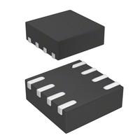
5PB1104CMGI developed by Renesas Electronics America Inc. belongs to the 1.8V to 3.3V high-performance LVCMOS clock buffer family. With a synchronous glitch-free output enable (OE) function, any potential intermediate incorrect output clock cycles can be eliminated when enabling or disabling outputs. Its specific characteristics make it well-suited for industrial applications and automotive applications including radar, lidar, and more.
Very low pin-to-pin skew: < 50ps
Very low additive jitter: < 50fs
Supply voltage: 1.8V to 3.3V
3.3V tolerant input clock
Integrated serial termination for 50Ω channel
Industrial applications
Automotive applications
| Factory Lead Time | 12 Weeks |
| Mounting Type | Surface Mount |
| Package / Case | 8-UFDFN |
| Operating Temperature | -40°C~85°C |
| Packaging | Strip |
| Part Status | Active |
| Moisture Sensitivity Level (MSL) | 1 (Unlimited) |
| Type | Fanout Buffer (Distribution) |
| Voltage - Supply | 1.71V~3.465V |
| Number of Circuits | 1 |
| Frequency (Max) | 200MHz |
| Input | LVCMOS |
| Ratio - Input:Output | 1:4 |
| Differential - Input:Output | No/No |
| RoHS Status | ROHS3 Compliant |

 5PB1104CMGI Datasheet
 +8613715157867