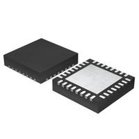
CDCLVD110ARHBRG4 OverviewThere is a case option of 32-VFQFN Exposed Pad available for this clock divider. There is a Tape & Reel (TR) packaged with it. Normal operation is limited to 1.1GHz. 32 terminations have been recorded. With a supply voltage of 2.5V, high efficiency is possible. As far as I can tell, it is mounted by Surface Mount. Electronic parts classified as Fanout Buffer (Distribution), Multiplexer are considered to be safety components. It is recommended to set the temperature to -40°C~85°C so the system can perform reliably. In order for it to function, a power source of 2.375V~2.625V V must be available. Surface Mount is placed within the way of this object. A pin count of 32 can be found on it. It is operated using the 32 pins. This is a member of the family of CDCLVD110. The gadget belongs to the 110 family of clock buffers. The maximum supply voltage (Vsup) has been set to 2.625V. As a rule, the supply voltage (Vsup) should be kept above 2.375V for normal operation. There is a default setting of output 10. In order to achieve maximum efficiency, the supply voltage should be kept at 2.5V. In addition, it consumes 35mA quiescent current and is unaffected by external factors. This method employs the TR packing method.
CDCLVD110ARHBRG4 Features32 terminations
The operating temperature of -40°C~85°C degrees
CDCLVD110ARHBRG4 ApplicationsThere are a lot of Texas Instruments
CDCLVD110ARHBRG4 Clock Buffers & Drivers applications.
Clock signal duplication
Clock signal format conversion
Clock signal level shifting
High performance communication system
Data center
Cloud computing
Network
High speed industry
High-end consumer electronics
Data communication
| Lifecycle Status | ACTIVE (Last Updated: 2 days ago) |
| Factory Lead Time | 12 Weeks |
| Contact Plating | Gold |
| Mount | Surface Mount |
| Mounting Type | Surface Mount |
| Package / Case | 32-VFQFN Exposed Pad |
| Number of Pins | 32 |
| Weight | 71.809342mg |
| Operating Temperature | -40°C~85°C |
| Packaging | Tape & Reel (TR) |
| JESD-609 Code | e4 |
| Pbfree Code | yes |
| Part Status | Active |
| Moisture Sensitivity Level (MSL) | 2 (1 Year) |
| Number of Terminations | 32 |
| Type | Fanout Buffer (Distribution), Multiplexer |
| Packing Method | TR |
| Voltage - Supply | 2.375V~2.625V |
| Terminal Position | QUAD |
| Peak Reflow Temperature (Cel) | 260 |
| Number of Functions | 1 |
| Supply Voltage | 2.5V |
| Base Part Number | CDCLVD110 |
| Pin Count | 32 |
| Number of Outputs | 10 |
| Operating Supply Voltage | 2.5V |
| Supply Voltage-Max (Vsup) | 2.625V |
| Supply Voltage-Min (Vsup) | 2.375V |
| Number of Circuits | 1 |
| Load Capacitance | 5pF |
| Propagation Delay | 3 ns |
| Quiescent Current | 35mA |
| Frequency (Max) | 1.1GHz |
| Family | 110 |
| Output Characteristics | 3-STATE |
| Input | LVDS |
| Ratio - Input:Output | 2:10 |
| Differential - Input:Output | Yes/Yes |
| Duty Cycle | 55 % |
| Height | 1mm |
| Length | 5mm |
| Width | 5mm |
| Thickness | 900μm |
| Radiation Hardening | No |
| RoHS Status | ROHS3 Compliant |
| Lead Free | Lead Free |

 CDCLVD110ARHBRG4 Datasheet
 +8613715157867