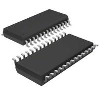
DS90LV110ATMTX OverviewThere is a case of 28-TSSOP (0.173, 4.40mm Width) in which it is packaged. Tape & Reel (TR) is the form in which it is packaged. It is recommended that the maximum value for normal operation is 200MHz. It has 28 terminations. With a voltage of 3.3V, high efficiency is possible. In this case, it is set up as Surface Mount. Electrical components classified as Fanout Buffer (Distribution) are classified as such. It is recommended to set the temperature to -40°C~85°C in order to ensure reliable performance. The clock switch should operate with a voltage of 3V~3.6VV. In this case, it is placed in the way of Surface Mount. The pin count is 28. As a result, it produces LVDS. A 28 pin is used for operation. The DS90LV110 family contains it. There is a 3.6V maximum supply voltage set (Vsup). Normal operation requires a voltage above 3V for the supply voltage (Vsup). The supply voltage should be kept at 3.3V for maximum efficiency.
DS90LV110ATMTX Features28 terminations
The operating temperature of -40°C~85°C degrees
DS90LV110ATMTX ApplicationsThere are a lot of Texas Instruments
DS90LV110ATMTX Clock Buffers & Drivers applications.
Car
Aviation
Medical instruments
Furniture
Machine made
Clock signal duplication
Clock signal format conversion
Clock signal level shifting
High performance communication system
Data center
| Mount | Surface Mount |
| Mounting Type | Surface Mount |
| Package / Case | 28-TSSOP (0.173, 4.40mm Width) |
| Number of Pins | 28 |
| Operating Temperature | -40°C~85°C |
| Packaging | Tape & Reel (TR) |
| JESD-609 Code | e0 |
| Pbfree Code | no |
| Part Status | Obsolete |
| Moisture Sensitivity Level (MSL) | 3 (168 Hours) |
| Number of Terminations | 28 |
| Type | Fanout Buffer (Distribution) |
| Terminal Finish | Tin/Lead (Sn/Pb) |
| Max Power Dissipation | 2.115W |
| Voltage - Supply | 3V~3.6V |
| Terminal Position | DUAL |
| Terminal Form | GULL WING |
| Peak Reflow Temperature (Cel) | 235 |
| Number of Functions | 1 |
| Supply Voltage | 3.3V |
| Terminal Pitch | 0.65mm |
| Base Part Number | DS90LV110 |
| Output | LVDS |
| Pin Count | 28 |
| Operating Supply Voltage | 3.3V |
| Supply Voltage-Max (Vsup) | 3.6V |
| Supply Voltage-Min (Vsup) | 3V |
| Number of Circuits | 1 |
| Propagation Delay | 3.9 ns |
| Turn On Delay Time | 3.9 ns |
| Frequency (Max) | 200MHz |
| Data Rate | 400 Mbps |
| Input | LVDS, LVPECL, PECL |
| Ratio - Input:Output | 1:10 |
| Power Consumption | 417W |
| Differential - Input:Output | Yes/Yes |
| Number of Drivers | 10 |
| Length | 9.7mm |
| Width | 4.4mm |
| Radiation Hardening | No |
| RoHS Status | Non-RoHS Compliant |
| Lead Free | Contains Lead |

 DS90LV110ATMTX Datasheet
 +8613715157867