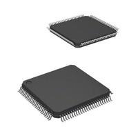
LCMXO2-640HC-4TG100C OverviewA 100-LQFP package contains it, and it is available for download. There are FIELD PROGRAMMABLE GATE ARRAY transistors in this type of FPGA. Its 78 I/Os help it transfer data more efficiently. A fundamental building block contains 640 logic elements or cells. Power is provided by a 2.5V-volt supply. The Surface Mount-slot connector on the FPGA module can be connected to the development board. Fpga chips operates at a voltage of 2.375V~3.465V and uses a battery to supply power. FPGAs belonging to the MachXO2 series are a type of FPGA that belong to the MachXO2 series of FPGAs. Operating temperatures should be maintained within the 0°C~85°C TJ range at all times when the unit is in use. During the installation of this device, 79 outputs were incorporated. A model of this FPGA is contained in Tray for the purpose of saving space. In total, there are a total of 100 terminations on fpga chips. Having a RAM bit size of 18432 means that this device will offer you a lot of memory. For related parts, use its base part number LCMXO2-640. A significant amount of RAM is allocated to this FPGA module to ensure that the program can operate normally. This cable has 100 pins and is designed to connect to a computer. 80 LABs/CLBs are integrated into this FPGA. Providing the FPGA is mounted in Surface Mount as per the specifications of the IC, then it should work perfectly according to its specifications. With a 2.5V supply voltage, designers can fully utilize the flexibility of the device. Power is supplied to the device by a 2.5/3.3V battery. In this FPGA module, there is a memory of 5.9kB available for storing applications and data. A frequency of 269MHz provides high efficiency. As most of the logic cells for the building blocks are 640 logic cells, it incorporates a lot of logic. During operation, it uses 1.84mA of supply current. CPLDs are built and controlled by a number of macrocells, which is the main part of the device. This memory is designed to store data efficiently and prevent resource conflicts.
LCMXO2-640HC-4TG100C Features78 I/Os
Up to 18432 RAM bits
100 LABs/CLBs
Operating from a frequency of 269MHz
LCMXO2-640HC-4TG100C ApplicationsThere are a lot of Lattice Semiconductor Corporation
LCMXO2-640HC-4TG100C FPGAs applications.
Integrating multiple SPLDs
Voice recognition
Cryptography
Filtering and communication encoding
Aerospace and Defense
Medical Electronics
Audio
Automotive
Consumer Electronics
Distributed Monetary Systems
| Factory Lead Time | 8 Weeks |
| Mount | Surface Mount |
| Mounting Type | Surface Mount |
| Package / Case | 100-LQFP |
| Number of Pins | 100 |
| Weight | 657.000198mg |
| Operating Temperature | 0°C~85°C TJ |
| Packaging | Tray |
| Series | MachXO2 |
| Published | 2000 |
| JESD-609 Code | e3 |
| Pbfree Code | yes |
| Part Status | Active |
| Moisture Sensitivity Level (MSL) | 3 (168 Hours) |
| Number of Terminations | 100 |
| ECCN Code | EAR99 |
| Terminal Finish | Matte Tin (Sn) |
| HTS Code | 8542.39.00.01 |
| Voltage - Supply | 2.375V~3.465V |
| Terminal Position | QUAD |
| Terminal Form | GULL WING |
| Peak Reflow Temperature (Cel) | 260 |
| Supply Voltage | 2.5V |
| Terminal Pitch | 0.5mm |
| Frequency | 269MHz |
| Time@Peak Reflow Temperature-Max (s) | 30 |
| Base Part Number | LCMXO2-640 |
| Number of Outputs | 79 |
| Operating Supply Voltage | 2.5V |
| Power Supplies | 2.5/3.3V |
| Memory Size | 5.9kB |
| Operating Supply Current | 1.84mA |
| Number of I/O | 78 |
| RAM Size | 2.3kB |
| Memory Type | FLASH |
| Propagation Delay | 7.24 ns |
| Programmable Logic Type | FIELD PROGRAMMABLE GATE ARRAY |
| Number of Logic Elements/Cells | 640 |
| Density | 147 kb |
| Total RAM Bits | 18432 |
| Number of LABs/CLBs | 80 |
| Number of Macro Cells | 320 |
| Number of Logic Cells | 640 |
| Length | 14mm |
| Height Seated (Max) | 1.6mm |
| Width | 14mm |
| REACH SVHC | No SVHC |
| Radiation Hardening | No |
| RoHS Status | ROHS3 Compliant |
| Lead Free | Lead Free |

 LCMXO2-640HC-4TG100C Datasheet
 +8613715157867