This SoC is built on ARM® Cortex®-M3 core processor(s).ARM® Cortex®-M3 core processor(s) are used in the construction of this SoC.Manufacturer assigns package 325-TFBGA, CSPBGA to this system on a chip.Users will enjoy reliable performance with this SoC chip, which has implemented 64KB RAM.The internal architecture of this SoC design is based on the MCU, FPGA technique.In the SmartFusion®2 series, this system on chip SoC is included.Typical operating temperatures for this SoC meaning should be 0°C~85°C TJ.Taking note of the fact that this SoC security combines FPGA - 25K Logic Modules is important.An advanced Tray package houses this SoC system on a chip.In total, this SoC part has 180 I/Os.Use a power supply with a voltage of 1.2V if possible.It is unsafe to operate the SoCs wireless at voltages above 1.26V.Power supplies of at least 1.14V are required.You can reconfigure FIELD PROGRAMMABLE GATE ARRAY to meet your specific design needs.A system on a chip benefits from having 325 terminations.A SoC chip like this can have 180 outputs.In order to operate system on chip, you will need 1.2V power supplies.This SoC chip has a total of 180 inputs that can be used.The logic SoC features 27696 logic cells.A flashing 256KB appears on it.This SoC processor also includes LG-MIN, WD-MIN.
ARM® Cortex®-M3 processor.64KB RAM.
Built on MCU, FPGA.
256KB extended flash.
LG-MIN, WD-MIN
There are a lot of Microsemi Corporation M2S025-1FCS325 System On Chip (SoC) applications.
Industrial robot
High-end PLC
Vending machines
POS Terminals
Measurement tools
Measurement testers
Networked sensors
Robotics
Central alarm system
Smart appliances
| Factory Lead Time | 10 Weeks |
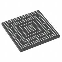
| Package / Case | 325-TFBGA, CSPBGA |
| Surface Mount | YES |
| Operating Temperature | 0°C~85°C TJ |
| Packaging | Tray |
| Series | SmartFusion®2 |
| Published | 2015 |
| JESD-609 Code | e0 |
| Part Status | Active |
| Moisture Sensitivity Level (MSL) | 3 (168 Hours) |
| Number of Terminations | 325 |
| Terminal Finish | Tin/Lead (Sn/Pb) |
| Additional Feature | LG-MIN, WD-MIN |
| HTS Code | 8542.39.00.01 |
| Terminal Position | BOTTOM |
| Terminal Form | BALL |
| Peak Reflow Temperature (Cel) | NOT SPECIFIED |
| Supply Voltage | 1.2V |
| Terminal Pitch | 0.5mm |
| Reach Compliance Code | not_compliant |
| Time@Peak Reflow Temperature-Max (s) | NOT SPECIFIED |
| JESD-30 Code | S-PBGA-B325 |
| Number of Outputs | 180 |
| Qualification Status | Not Qualified |
| Supply Voltage-Max (Vsup) | 1.26V |
| Power Supplies | 1.2V |
| Supply Voltage-Min (Vsup) | 1.14V |
| Number of I/O | 180 |
| Speed | 166MHz |
| RAM Size | 64KB |
| Core Processor | ARM® Cortex®-M3 |
| Peripherals | DDR, PCIe, SERDES |
| Connectivity | CANbus, Ethernet, I2C, SPI, UART/USART, USB |
| Architecture | MCU, FPGA |
| Number of Inputs | 180 |
| Programmable Logic Type | FIELD PROGRAMMABLE GATE ARRAY |
| Primary Attributes | FPGA - 25K Logic Modules |
| Number of Logic Cells | 27696 |
| Flash Size | 256KB |
| Length | 11mm |
| Height Seated (Max) | 1.01mm |
| Width | 11mm |
| RoHS Status | Non-RoHS Compliant |

 M2S025-1FCS325 Datasheet
 +8613715157867