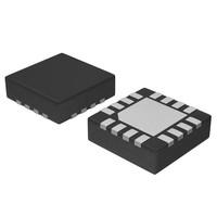
NB3L202KMNG OverviewIt is available in the case 16-VFQFN Exposed Pad for this cut smart buffer. It is available in the case Tube. There is a maximum value of 350MHz for normal operation. There are 16 terminations in it. Using a supply voltage of 2.5V allows for high efficiency. Consequently, it will be mounted by Surface Mount. There is a classification of Fanout Buffer (Distribution) for this electronic part. The temperature should be set to -40°C~85°C to ensure reliable performance. This circuit clock should be able to operate on a power supply of 2.375V~3.63V volts. There is an output of HCSL. It is part of the NB3 family of electronic buffer ICs. It's set to 2.625V for the maximum supply voltage (Vsup). To ensure normal operation of the cut smart buffer, the supply voltage (Vsup) should always be kept above 2.375V. It is also possible to obtain ALSO OPERATES AT 2.97 TO 3.63 V SUPPLY by using this gadget.
NB3L202KMNG Features16 terminations
The operating temperature of -40°C~85°C degrees
NB3L202KMNG ApplicationsThere are a lot of ON Semiconductor
NB3L202KMNG Clock Buffers & Drivers applications.
High performance communication system
Data center
Cloud computing
Network
High speed industry
High-end consumer electronics
Data communication
Telecommunications
Computing
Medical imaging
| Lifecycle Status | ACTIVE (Last Updated: 1 day ago) |
| Factory Lead Time | 5 Weeks |
| Mounting Type | Surface Mount |
| Package / Case | 16-VFQFN Exposed Pad |
| Surface Mount | YES |
| Operating Temperature | -40°C~85°C |
| Packaging | Tube |
| Published | 2006 |
| JESD-609 Code | e3 |
| Pbfree Code | yes |
| Part Status | Active |
| Moisture Sensitivity Level (MSL) | 1 (Unlimited) |
| Number of Terminations | 16 |
| Type | Fanout Buffer (Distribution) |
| Terminal Finish | Tin (Sn) |
| Additional Feature | ALSO OPERATES AT 2.97 TO 3.63 V SUPPLY |
| Voltage - Supply | 2.375V~3.63V |
| Terminal Position | QUAD |
| Terminal Form | NO LEAD |
| Peak Reflow Temperature (Cel) | NOT SPECIFIED |
| Number of Functions | 1 |
| Supply Voltage | 2.5V |
| Terminal Pitch | 0.5mm |
| Time@Peak Reflow Temperature-Max (s) | NOT SPECIFIED |
| Output | HCSL |
| Supply Voltage-Max (Vsup) | 2.625V |
| Supply Voltage-Min (Vsup) | 2.375V |
| Number of Circuits | 1 |
| Frequency (Max) | 350MHz |
| Family | NB3 |
| Input | HCSL, LVCMOS, LVDS, LVPECL, LVTTL |
| Ratio - Input:Output | 1:2 |
| Differential - Input:Output | Yes/Yes |
| fmax-Min | 350 MHz |
| Same Edge Skew-Max (tskwd) | 0.02 ns |
| Length | 3mm |
| Width | 3mm |
| RoHS Status | ROHS3 Compliant |

 NB3L202KMNG Datasheet
 +8613715157867