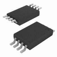
NB3V1103CDTR2G OverviewIt is package in 8-TSSOP (0.173, 4.40mm Width) case. It is packaged as a Tape & Reel (TR). In normal operation, 250MHz is the maximum value. A total of 8 terminations can be found in it. It is possible to achieve high efficiency with a 1.8V supply voltage. The mount is made up of Surface Mount. Electronic components classified as Fanout Buffer (Distribution) fall into this category. Setting the temperature to -40°C~105°C ensures reliable performance. 1.71V~3.6V V power should work with it. As a result, it is placed in the way of Surface Mount. It belongs to the family of electronic gadgets known as NB3V. This output has 3 true outputs. It is also possible to obtain ALSO OPERATES AT 2.5V AND 3.3V VCC NOMINAL SUPPLY when using this gadget.
NB3V1103CDTR2G Features8 terminations
The operating temperature of -40°C~105°C degrees
NB3V1103CDTR2G ApplicationsThere are a lot of ON Semiconductor
NB3V1103CDTR2G Clock Buffers & Drivers applications.
Furniture
Machine made
Clock signal duplication
Clock signal format conversion
Clock signal level shifting
High performance communication system
Data center
Cloud computing
Network
High speed industry
| Lifecycle Status | ACTIVE (Last Updated: 2 days ago) |
| Factory Lead Time | 8 Weeks |
| Mount | Surface Mount |
| Mounting Type | Surface Mount |
| Package / Case | 8-TSSOP (0.173, 4.40mm Width) |
| Operating Temperature | -40°C~105°C |
| Packaging | Tape & Reel (TR) |
| Published | 2008 |
| JESD-609 Code | e3 |
| Pbfree Code | yes |
| Part Status | Active |
| Moisture Sensitivity Level (MSL) | 1 (Unlimited) |
| Number of Terminations | 8 |
| Type | Fanout Buffer (Distribution) |
| Terminal Finish | Tin (Sn) |
| Additional Feature | ALSO OPERATES AT 2.5V AND 3.3V VCC NOMINAL SUPPLY |
| Voltage - Supply | 1.71V~3.6V |
| Terminal Position | DUAL |
| Terminal Form | GULL WING |
| Peak Reflow Temperature (Cel) | NOT SPECIFIED |
| Number of Functions | 1 |
| Supply Voltage | 1.8V |
| Terminal Pitch | 0.65mm |
| Time@Peak Reflow Temperature-Max (s) | NOT SPECIFIED |
| JESD-30 Code | R-PDSO-G8 |
| Number of Circuits | 1 |
| Frequency (Max) | 250MHz |
| Family | NB3V |
| Output Characteristics | 3-STATE |
| Input | LVCMOS |
| Ratio - Input:Output | 1:3 |
| Differential - Input:Output | No/No |
| Propagation Delay (tpd) | 3.5 ns |
| fmax-Min | 250 MHz |
| Same Edge Skew-Max (tskwd) | 0.075 ns |
| Number of True Outputs | 3 |
| Length | 4.4mm |
| Width | 3mm |
| RoHS Status | ROHS3 Compliant |
| Lead Free | Lead Free |

 NB3V1103CDTR2G Datasheet
 +8613715157867