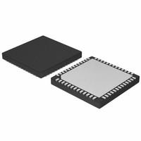
NB7L111MMNR2 OverviewThere is a case available for the cut smart buffer in 52-VFQFN Exposed Pad. This package is packaged in the form of a Tape & Reel (TR). For normal operation, 5.5GHz is the maximum value. It has 52 terminations in it, which means that it is terminated. Supply voltages of 2.5V are capable of achieving high efficiency. In this case, it will be mounted by Surface Mount. A classification of Fanout Buffer (Distribution), Multiplexer, Data is assigned to this electronic part. Setting the temperature to -40°C~85°C will ensure reliable performance. Ideally, it should be able to operate from 2.375V~3.465V volts. It has been positioned in the way of Surface Mount. There are 52 pins on the clock buffer. There is a value of CML as the output. During operation, 52 pins are used. As a member of the NB7L111M family, it falls under that category. A member of the 7L family, this clock buffer is a digital camera. Vsup is set to 2.625V as the maximum supply voltage. As a general rule, the supply voltage (Vsup) should be maintained above 2.375V. The timeing clock is powered by a power supply of 2.5/3.3V volts. By utilizing this gadget, one can also obtain ALSO OPERATES WITH 3.3V SUPPLY.
NB7L111MMNR2 Features52 terminations
The operating temperature of -40°C~85°C degrees
NB7L111MMNR2 ApplicationsThere are a lot of ON Semiconductor
NB7L111MMNR2 Clock Buffers & Drivers applications.
Clock signal format conversion
Clock signal level shifting
High performance communication system
Data center
Cloud computing
Network
High speed industry
High-end consumer electronics
Data communication
Telecommunications
| Mount | Surface Mount |
| Mounting Type | Surface Mount |
| Package / Case | 52-VFQFN Exposed Pad |
| Number of Pins | 52 |
| Operating Temperature | -40°C~85°C |
| Packaging | Tape & Reel (TR) |
| Published | 2007 |
| JESD-609 Code | e0 |
| Part Status | Obsolete |
| Moisture Sensitivity Level (MSL) | 1 (Unlimited) |
| Number of Terminations | 52 |
| Type | Fanout Buffer (Distribution), Multiplexer, Data |
| Terminal Finish | Tin/Lead (Sn/Pb) |
| Additional Feature | ALSO OPERATES WITH 3.3V SUPPLY |
| Voltage - Supply | 2.375V~3.465V |
| Terminal Position | QUAD |
| Number of Functions | 1 |
| Supply Voltage | 2.5V |
| Terminal Pitch | 0.5mm |
| Base Part Number | NB7L111M |
| Output | CML |
| Pin Count | 52 |
| Supply Voltage-Max (Vsup) | 2.625V |
| Power Supplies | 2.5/3.3V |
| Supply Voltage-Min (Vsup) | 2.375V |
| Number of Circuits | 1 |
| Frequency (Max) | 5.5GHz |
| Family | 7L |
| Data Rate | 6 Gbps |
| Input | CML, LVCMOS, LVDS, LVNECL, LVPECL, LVTTL |
| Ratio - Input:Output | 2:10 |
| Differential - Input:Output | Yes/Yes |
| Prop. Delay@Nom-Sup | 0.28 ns |
| Propagation Delay (tpd) | 0.28 ns |
| Same Edge Skew-Max (tskwd) | 0.02 ns |
| Length | 8mm |
| Width | 8mm |
| Radiation Hardening | No |
| RoHS Status | Non-RoHS Compliant |
| Lead Free | Contains Lead |

 NB7L111MMNR2 Datasheet
 +8613715157867