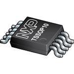
PCA9615DP OverviewSpeaking of types, this is a typical Buffer.The pinout of the power buffer starts from 10 pins it has.
PCA9615DP FeaturesPCA9615DP ApplicationsThere are a lot of NXP Semiconductors
PCA9615DP Signal Buffers, Repeaters, Splitters applications.
Data or Clock Signal Amplification
PECL-to-LVDS Translation
Cellular Phone Base Stations
Add/Drop Muxes
Digital Crossconnects
Network Switches/Routers
Backplane Interconnect
Clock Distribution
Protection Switching
Loopback
| ECCN (US) | EAR99 |
| Input Signal Type | I2C |
| Typical Input Capacitance (pF) | 6 |
| Minimum Operating Supply Voltage (V) | 3|2.3 |
| Maximum Operating Supply Voltage (V) | 5.5 |
| Typical Operating Supply Voltage (V) | 5|3.3|2.5 |
| Maximum Supply Current (mA) | 91 |
| Maximum Power Dissipation (mW) | 100 |
| Minimum Operating Temperature (°C) | -40 |
| Maximum Operating Temperature (°C) | 85 |
| Standard Package Name | SOP |
| Supplier Package | TSSOP |
| Mounting | Surface Mount |
| Package Height | 0.95(Max) |
| Package Length | 3.1(Max) |
| Package Width | 3.1(Max) |
| PCB changed | 10 |
| Lead Shape | Gull-wing |
| Part Status | Active |
| Type | Buffer |
| Pin Count | 10 |
| RoHS Status | RoHS Compliant |

 PCA9615DP Datasheet
 +8613715157867