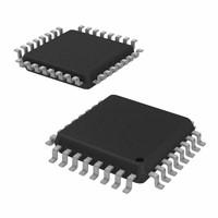
PCK9448BD,157 OverviewIt is available in the case 32-LQFP for this cut smart buffer. It is available in the case Tray. There is a maximum value of 350MHz for normal operation. There are 32 terminations in it. Using a supply voltage of 2.5V allows for high efficiency. Consequently, it will be mounted by Surface Mount. There is a classification of Fanout Buffer (Distribution), Multiplexer for this electronic part. The temperature should be set to -40°C~85°C to ensure reliable performance. This circuit clock should be able to operate on a power supply of 2.375V~3.465V volts. It has a number of pins of 32. There is an output of LVCMOS. There is a family of objects known as the PCK9448. It's set to 2.625V for the maximum supply voltage (Vsup). To ensure normal operation of the cut smart buffer, the supply voltage (Vsup) should always be kept above 2.375V. Power for the clock buffer comes from a 2.5/3.3V volt supply. It is also possible to obtain ALSO OPERATES AT 3.3V SUPPLY by using this gadget.
PCK9448BD,157 Features32 terminations
The operating temperature of -40°C~85°C degrees
PCK9448BD,157 ApplicationsThere are a lot of NXP USA Inc.
PCK9448BD,157 Clock Buffers & Drivers applications.
High performance communication system
Data center
Cloud computing
Network
High speed industry
High-end consumer electronics
Data communication
Telecommunications
Computing
Medical imaging
| Mounting Type | Surface Mount |
| Package / Case | 32-LQFP |
| Surface Mount | YES |
| Operating Temperature | -40°C~85°C |
| Packaging | Tray |
| Published | 2005 |
| Part Status | Obsolete |
| Moisture Sensitivity Level (MSL) | 1 (Unlimited) |
| Number of Terminations | 32 |
| Type | Fanout Buffer (Distribution), Multiplexer |
| Additional Feature | ALSO OPERATES AT 3.3V SUPPLY |
| Voltage - Supply | 2.375V~3.465V |
| Terminal Position | QUAD |
| Terminal Form | GULL WING |
| Number of Functions | 1 |
| Supply Voltage | 2.5V |
| Terminal Pitch | 0.8mm |
| Base Part Number | PCK9448 |
| Output | LVCMOS |
| Pin Count | 32 |
| JESD-30 Code | S-PQFP-G32 |
| Qualification Status | Not Qualified |
| Supply Voltage-Max (Vsup) | 2.625V |
| Power Supplies | 2.5/3.3V |
| Supply Voltage-Min (Vsup) | 2.375V |
| Number of Circuits | 1 |
| Frequency (Max) | 350MHz |
| Input | LVCMOS, LVPECL |
| Ratio - Input:Output | 2:12 |
| Differential - Input:Output | Yes/Yes |
| Prop. Delay@Nom-Sup | 4.4 ns |
| Propagation Delay (tpd) | 4.4 ns |
| fmax-Min | 350 MHz |
| Length | 7mm |
| Width | 7mm |
| RoHS Status | ROHS3 Compliant |

 PCK9448BD,157 Datasheet
 +8613715157867