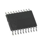
PI6C4911506LIEX OverviewIt is package in 20-TSSOP (0.173, 4.40mm Width) case. It is packaged as a Tape & Reel (TR). In normal operation, 1.5GHz is the maximum value. A total of 20 terminations can be found in it. It is possible to achieve high efficiency with a 2.5V supply voltage. The mount is made up of Surface Mount. Electronic components classified as Fanout Buffer (Distribution) fall into this category. Setting the temperature to -40°C~85°C TA ensures reliable performance. 2.375V~2.625V 3V~3.6V V power should work with it. The output of it is LVPECL. It belongs to the family of electronic gadgets known as 6C. In this case, the maximum supply voltage (Vsup) is set to 2.625V. In order to maintain normal operation, the supply voltage (Vsup) should be maintained above 2.375V. It is also possible to obtain ALSO OPERATES AT 3 TO 3.6 V SUPPLY when using this gadget.
PI6C4911506LIEX Features20 terminations
The operating temperature of -40°C~85°C TA degrees
PI6C4911506LIEX ApplicationsThere are a lot of Diodes Incorporated
PI6C4911506LIEX Clock Buffers & Drivers applications.
Furniture
Machine made
Clock signal duplication
Clock signal format conversion
Clock signal level shifting
High performance communication system
Data center
Cloud computing
Network
High speed industry
| Factory Lead Time | 20 Weeks |
| Mounting Type | Surface Mount |
| Package / Case | 20-TSSOP (0.173, 4.40mm Width) |
| Surface Mount | YES |
| Operating Temperature | -40°C~85°C TA |
| Packaging | Tape & Reel (TR) |
| Part Status | Active |
| Moisture Sensitivity Level (MSL) | 1 (Unlimited) |
| Number of Terminations | 20 |
| ECCN Code | EAR99 |
| Type | Fanout Buffer (Distribution) |
| Additional Feature | ALSO OPERATES AT 3 TO 3.6 V SUPPLY |
| Voltage - Supply | 2.375V~2.625V 3V~3.6V |
| Terminal Position | DUAL |
| Terminal Form | GULL WING |
| Peak Reflow Temperature (Cel) | NOT SPECIFIED |
| Number of Functions | 1 |
| Supply Voltage | 2.5V |
| Terminal Pitch | 0.65mm |
| Time@Peak Reflow Temperature-Max (s) | NOT SPECIFIED |
| Output | LVPECL |
| JESD-30 Code | R-PDSO-G20 |
| Supply Voltage-Max (Vsup) | 2.625V |
| Supply Voltage-Min (Vsup) | 2.375V |
| Number of Circuits | 1 |
| Frequency (Max) | 1.5GHz |
| Family | 6C |
| Input | CMOS, LVDS, LVPECL |
| Ratio - Input:Output | 1:6 |
| Differential - Input:Output | Yes/Yes |
| Propagation Delay (tpd) | 0.7 ns |
| Same Edge Skew-Max (tskwd) | 0.05 ns |
| Length | 6.5mm |
| Width | 4.4mm |
| RoHS Status | ROHS3 Compliant |

 PI6C4911506LIEX Datasheet
 +8613715157867