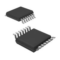
SN65LVDS105PWG4 OverviewThere is a package of 16-TSSOP (0.173, 4.40mm Width) for easy transportation of this power buffer.Currently, this power buffer is available for shipping in Tube packages.The Surface Mount universal mout allows for easy adaptability to a variety of situations.It is important to note that this is a typical Buffer, Multiplexer type.The op amp buffer uses a voltage of 3V~3.6V volts for its operation.In order to maintain the output quality, 1 x 1:4 channels cooperate with each other.As a result, LVTTL input can be facilitated.There should be a setting of -40°C~85°C for the operating temperature in order to avoid any malfunctions.There are more pin-to-pin solutions available for your special needs if you search with the letter "65LVDS105".There is a 16 terminal on the op amp buffer, which can be seen in the picture below.During reflow, it reaches a peak temperature of 260.Powered by 3.3V voltage, the splitter can be used to accomplish a wide variety of demanding tasks.The pinout of a Power buffer begins with the 16 pins of the Power buffer that it possesses.There is a LVDS output from it.16 pins are present on the op amp buffers.For mounting on PCBs or other boards, it has a Surface Mount.A voltage of 23mA is required to operate this power buffer.Operating voltage 3.3V is required for normal operation.Using a 1-Bit receiver, it transmits and receives data.It dissipates a maximum of 774mW watts of power.A nominal supply current of 23mA is recommended for normal operation of the splitter.There are a total of 4 outputs supported.
SN65LVDS105PWG4 Features1 x 1:4 channels.
1-Bit receiver.
4 outputs.
SN65LVDS105PWG4 ApplicationsThere are a lot of Texas Instruments
SN65LVDS105PWG4 Signal Buffers, Repeaters, Splitters applications.
PECL-to-LVDS Translation
Cellular Phone Base Stations
Add/Drop Muxes
Digital Crossconnects
Network Switches/Routers
Backplane Interconnect
Clock Distribution
Protection Switching
Loopback
Clock Distribution
| Lifecycle Status | ACTIVE (Last Updated: 1 week ago) |
| Factory Lead Time | 6 Weeks |
| Mount | Surface Mount |
| Mounting Type | Surface Mount |
| Package / Case | 16-TSSOP (0.173, 4.40mm Width) |
| Number of Pins | 16 |
| Weight | 59.987591mg |
| Operating Temperature | -40°C~85°C |
| Packaging | Tube |
| JESD-609 Code | e4 |
| Pbfree Code | yes |
| Part Status | Active |
| Moisture Sensitivity Level (MSL) | 1 (Unlimited) |
| Number of Terminations | 16 |
| ECCN Code | EAR99 |
| Type | Buffer, Multiplexer |
| Terminal Finish | Nickel/Palladium/Gold (Ni/Pd/Au) |
| Max Power Dissipation | 774mW |
| Voltage - Supply | 3V~3.6V |
| Terminal Position | DUAL |
| Terminal Form | GULL WING |
| Peak Reflow Temperature (Cel) | 260 |
| Number of Functions | 1 |
| Supply Voltage | 3.3V |
| Frequency | 400MHz |
| Base Part Number | 65LVDS105 |
| Output | LVDS |
| Pin Count | 16 |
| Number of Outputs | 4 |
| Operating Supply Voltage | 3.3V |
| Number of Channels | 1 x 1:4 |
| Operating Supply Current | 23mA |
| Nominal Supply Current | 23mA |
| Power Dissipation | 774mW |
| Propagation Delay | 4.2 ns |
| Turn On Delay Time | 4.2 ns |
| Input | LVTTL |
| Driver Number of Bits | 4 |
| Receiver Number of Bits | 1 |
| Receive Delay-Max | 3.5 ns |
| Data Rate (Max) | 400Mbps |
| Transmit Delay-Max | 3.5 ns |
| Supply Voltage1-Nom | 3.3V |
| Out Swing-Min | 2 V |
| Delay Time | 2.2ns |
| Capacitance - Input | 3pF |
| Height | 1.2mm |
| Length | 5mm |
| Width | 4.4mm |
| Thickness | 1mm |
| Radiation Hardening | No |
| RoHS Status | ROHS3 Compliant |
| Lead Free | Lead Free |


 +8613715157867