8SLVD1208NBGI/W OverviewThere is a case of 28-VFQFN Exposed Pad in which it is packaged. Tape & Reel (TR) is the form in which it is packaged. It is recommended that the maximum value for normal operation is 2GHz. In this case, it is set up as Surface Mount. Electrical components classified as Fanout Buffer (Distribution), Multiplexer are classified as such. It is recommended to set the temperature to -40°C~85°C in order to ensure reliable performance. The clock switch should operate with a voltage of 2.375V~2.625VV. As a result, it produces LVDS.
8SLVD1208NBGI/W FeaturesThe operating temperature of -40°C~85°C degrees
8SLVD1208NBGI/W ApplicationsThere are a lot of Renesas Electronics America Inc.
8SLVD1208NBGI/W Clock Buffers & Drivers applications.
Car
Aviation
Medical instruments
Furniture
Machine made
Clock signal duplication
Clock signal format conversion
Clock signal level shifting
High performance communication system
Data center
| Mounting Type | Surface Mount |
| Package / Case | 28-VFQFN Exposed Pad |
| Operating Temperature | -40°C~85°C |
| Packaging | Tape & Reel (TR) |
| Part Status | Active |
| Moisture Sensitivity Level (MSL) | 1 (Unlimited) |
| Type | Fanout Buffer (Distribution), Multiplexer |
| Voltage - Supply | 2.375V~2.625V |
| Output | LVDS |
| Number of Circuits | 1 |
| Frequency (Max) | 2GHz |
| Input | LVDS, LVPECL |
| Ratio - Input:Output | 2:8 |
| Differential - Input:Output | Yes/Yes |
| RoHS Status | ROHS3 Compliant |
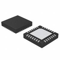

 8SLVD1208NBGI/W Datasheet
 +8613715157867