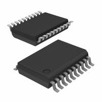
CY2CC810OXI OverviewA 20-SSOP (0.209, 5.30mm Width) case is used for packaging. A Tube is used to package it. Under normal circumstances, 650MHz is the maximum value. In it, there are 20 terminations. Supply voltages of 2.5V allow for high efficiency. A mount of Surface Mount has been applied to it. This electronic component falls under the classification of Fanout Buffer (Distribution). Temperature -40°C~85°C is recommended for reliable performance. With a 2.375V~3.465VV power source, it should work. There are 20 pins on timeing clock. There is AVCMOS output from clock driver. Operation is performed with 20 pins. It belongs to the family CY2CC810. A member of the 2CC family, this gadget is a timeing clock. In this case, Vsup will be set to 2.625V (decimal). In order for the supply voltage (Vsup) to stay above 2.375V, it should be kept as high as possible. By default, the output is set to 10. It is recommended to keep the supply voltage at 3.3V to maximize efficiency. There is no external influence on it, as it consumes 25mA quiescent current.
CY2CC810OXI Features20 terminations
The operating temperature of -40°C~85°C degrees
CY2CC810OXI ApplicationsThere are a lot of Cypress Semiconductor Corp
CY2CC810OXI Clock Buffers & Drivers applications.
Medical instruments
Furniture
Machine made
Clock signal duplication
Clock signal format conversion
Clock signal level shifting
High performance communication system
Data center
Cloud computing
Network
| Factory Lead Time | 8 Weeks |
| Contact Plating | Gold, Tin |
| Mounting Type | Surface Mount |
| Package / Case | 20-SSOP (0.209, 5.30mm Width) |
| Surface Mount | YES |
| Number of Pins | 20 |
| Operating Temperature | -40°C~85°C |
| Packaging | Tube |
| Published | 2002 |
| JESD-609 Code | e3 |
| Pbfree Code | yes |
| Part Status | Obsolete |
| Moisture Sensitivity Level (MSL) | 3 (168 Hours) |
| Number of Terminations | 20 |
| ECCN Code | EAR99 |
| Type | Fanout Buffer (Distribution) |
| Terminal Finish | Matte Tin (Sn) |
| Max Power Dissipation | 750mW |
| Voltage - Supply | 2.375V~3.465V |
| Terminal Position | DUAL |
| Terminal Form | GULL WING |
| Peak Reflow Temperature (Cel) | 260 |
| Number of Functions | 1 |
| Supply Voltage | 2.5V |
| Terminal Pitch | 0.65mm |
| Time@Peak Reflow Temperature-Max (s) | 30 |
| Base Part Number | CY2CC810 |
| Output | AVCMOS |
| Pin Count | 20 |
| Number of Outputs | 10 |
| Operating Supply Voltage | 3.3V |
| Supply Voltage-Max (Vsup) | 2.625V |
| Supply Voltage-Min (Vsup) | 2.375V |
| Number of Circuits | 1 |
| Power Dissipation | 750mW |
| Propagation Delay | 3.5 ns |
| Quiescent Current | 25mA |
| Turn On Delay Time | 3.5 ns |
| Frequency (Max) | 650MHz |
| Family | 2CC |
| Input | LVCMOS |
| Ratio - Input:Output | 1:10 |
| Differential - Input:Output | No/No |
| Same Edge Skew-Max (tskwd) | 0.38 ns |
| Height | 1.85mm |
| Length | 7.4mm |
| Width | 5.6mm |
| Radiation Hardening | No |
| RoHS Status | ROHS3 Compliant |
| Lead Free | Lead Free |

 CY2CC810OXI Datasheet
 +8613715157867