CY7B9911V-5JC OverviewThe Tube method is used for packaging clock ICs. As part of the 32-LCC (J-Lead) package, this clock generator is embedded. This clock generator ic can sustain 220 degrees of temperature during reflowing. There are 32 terminations found in this file. To operate this time clock generator, 3.3V voltage should be applied. In this clock generator, LVTTL is used as the input to the clock. For a full understanding of the electronic part's performance, 1 circuits are implemented. An up to 110MHz frequency is provided by this clock-based RF synthesizer. The Surface Mount allows the electrical component to be installed conveniently on the panel. 3.63V would be the maximum supply voltage for this clock generator. In order to maintain safety, this frequency generator should be supplied with voltages above 2.97V. In terms of supply voltage, RF synthesizer works with 3V~3.6V. Test statistics estimate a temperature of 0°C~70°C, which should be set as the ambient temperature. It has been classified as a Fanout Buffer (Distribution), Zero Delay Buffer electronic part, which means that it is a semiconductor. It is a 32-bit clock PLL designed specifically for microprocessors. It is possible to find its related electronic parts by searching for the base part number CY7B9911. There are 32 pins on the frequency generators that are available for use. Supply voltage 3.3V is what clock generator can handle. RoboClock+™ series electronic parts are used in this part. 8 signal outputs are provided for enhancing output frequency as much as possible. Low timing skew is offered by this RF synthesizer at maximum 0.7 ns. By searching for parts that belong to the 7B family, you can find electronic parts that are similar.
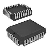
CY7B9911V-5JC FeaturesAvailable in the 32-LCC (J-Lead)
Supply voltage of 3.3V
Operating supply voltage of 3.3V
CY7B9911V-5JC ApplicationsThere are a lot of Cypress Semiconductor Corp
CY7B9911V-5JC Clock Generators applications.
Wireless base station for LTE, LTE-advanced
Picocells, femtocells and small cells
Sampling clocks for ADC and DAC
1 Gigabit Ethernet
10 Gigabit Ethernet
FPGA and processor clocks
Line cards used in telephone exchange
Fiber Channel
PCI express cards
Infotainment systems
| Mounting Type | Surface Mount |
| Package / Case | 32-LCC (J-Lead) |
| Surface Mount | YES |
| Number of Pins | 32 |
| Operating Temperature | 0°C~70°C |
| Packaging | Tube |
| Series | RoboClock+™ |
| Published | 1996 |
| JESD-609 Code | e0 |
| Pbfree Code | no |
| Part Status | Obsolete |
| Moisture Sensitivity Level (MSL) | 3 (168 Hours) |
| Number of Terminations | 32 |
| ECCN Code | EAR99 |
| Type | Fanout Buffer (Distribution), Zero Delay Buffer |
| Terminal Finish | Tin/Lead (Sn/Pb) |
| Voltage - Supply | 3V~3.6V |
| Terminal Position | QUAD |
| Terminal Form | J BEND |
| Peak Reflow Temperature (Cel) | 220 |
| Number of Functions | 1 |
| Supply Voltage | 3.3V |
| Base Part Number | CY7B9911 |
| Pin Count | 32 |
| Number of Outputs | 8 |
| Operating Supply Voltage | 3.3V |
| Supply Voltage-Max (Vsup) | 3.63V |
| Supply Voltage-Min (Vsup) | 2.97V |
| Number of Circuits | 1 |
| Power Dissipation | 104mW |
| Frequency (Max) | 110MHz |
| Family | 7B |
| Input | LVTTL |
| Ratio - Input:Output | 1:8 |
| Max I(ol) | 0.035 A |
| PLL | Yes |
| Differential - Input:Output | No/No |
| Prop. Delay@Nom-Sup | 0.5 ns |
| Propagation Delay (tpd) | 0.5 ns |
| Divider/Multiplier | Yes/Yes |
| Same Edge Skew-Max (tskwd) | 0.7 ns |
| Height Seated (Max) | 3.556mm |
| Radiation Hardening | No |
| RoHS Status | Non-RoHS Compliant |
| Lead Free | Contains Lead |


 +8613715157867